palikari
Junior Member level 2
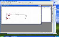
PSPICE error: "Design not annotated"
When trying to simulate this circuit, I get this error. Apparently it's before the netlist is created, because when I try to view netlist it doesn't do anything. Anyone know why I'm getting this error?
Creating PSpice Netlist
Writing PSpice Flat Netlist C:\PRACTICE-SCHEMATIC1.net
ERROR [NET0018] Design is not annotated.
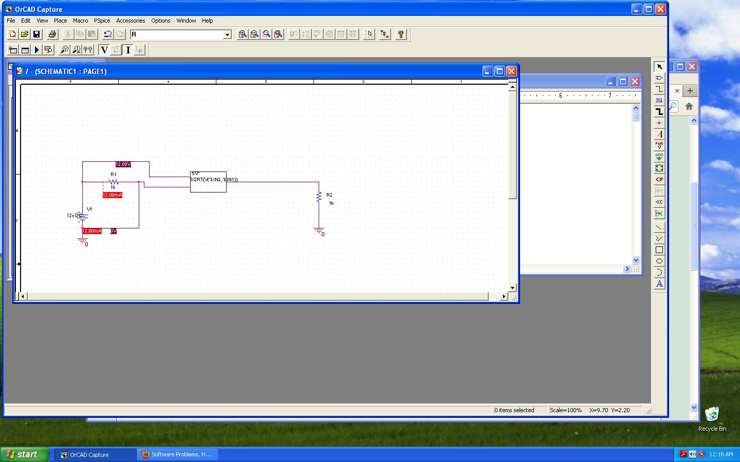
This is an ABM that is supposed to take SQRT of the voltage between the 2 inputs and multiply it by 5.
It is straight from the Orcad user's guide.
In this case, 5*SQRT(12).
As far as the 1k load resistor R2, I only put that there because I had to connect something to the end terminal. Wasn't sure what else to connect. Any ideas on that as well?
- - - Updated - - -
ok the above was for transient analysis. I tried doing a DC Sweep of the voltage source instead, and this time I got an error, but it showed me the netlist. Anyone know why the output needs 2 connections, and what else I should connect? Here is the output file text:
**** RESUMING practice-schematic1-myprof.sim.cir ****
.INC "practice-SCHEMATIC1.als"
**** INCLUDING practice-SCHEMATIC1.als ****
.ALIASES
V_V1 V1(+=N00019 -=0 )
R_R3 R3(1=0 2=N02045 )
R_R1 R1(1=N00019 2=0 )
**** RESUMING practice-schematic1-myprof.sim.cir ****
.END
ERROR -- Less than 2 connections at node N02045
- - - Updated - - -
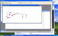
Ok, I solved the original error. Now my problem is a different one. Although I can simulate without errors, the output of that ABM block is 0.
In the output log it says:
"No sumulation data for marker 'V(ABM2?:OUT)' "
And the plot screen shows up but there is no plot on it. I have changed my original expression to a simple addition of the 2 inputs. The schematic is attached. Notice the output shows 0 V as well. Anyone know the problem here?
When trying to simulate this circuit, I get this error. Apparently it's before the netlist is created, because when I try to view netlist it doesn't do anything. Anyone know why I'm getting this error?
Creating PSpice Netlist
Writing PSpice Flat Netlist C:\PRACTICE-SCHEMATIC1.net
ERROR [NET0018] Design is not annotated.
This is an ABM that is supposed to take SQRT of the voltage between the 2 inputs and multiply it by 5.
It is straight from the Orcad user's guide.
In this case, 5*SQRT(12).
As far as the 1k load resistor R2, I only put that there because I had to connect something to the end terminal. Wasn't sure what else to connect. Any ideas on that as well?
- - - Updated - - -
ok the above was for transient analysis. I tried doing a DC Sweep of the voltage source instead, and this time I got an error, but it showed me the netlist. Anyone know why the output needs 2 connections, and what else I should connect? Here is the output file text:
**** RESUMING practice-schematic1-myprof.sim.cir ****
.INC "practice-SCHEMATIC1.als"
**** INCLUDING practice-SCHEMATIC1.als ****
.ALIASES
V_V1 V1(+=N00019 -=0 )
R_R3 R3(1=0 2=N02045 )
R_R1 R1(1=N00019 2=0 )
**** RESUMING practice-schematic1-myprof.sim.cir ****
.END
ERROR -- Less than 2 connections at node N02045
- - - Updated - - -
Ok, I solved the original error. Now my problem is a different one. Although I can simulate without errors, the output of that ABM block is 0.
In the output log it says:
"No sumulation data for marker 'V(ABM2?:OUT)' "
And the plot screen shows up but there is no plot on it. I have changed my original expression to a simple addition of the 2 inputs. The schematic is attached. Notice the output shows 0 V as well. Anyone know the problem here?
