Continue to Site

Welcome to EDAboard.com

Welcome to our site! EDAboard.com is an international Electronics Discussion Forum focused on EDA software, circuits, schematics, books, theory, papers, asic, pld, 8051, DSP, Network, RF, Analog Design, PCB, Service Manuals... and a whole lot more! To participate you need to register. Registration is free. Click here to register now.

Resistor and Capacitor in feedback path of unity gain amplifier

Status
Not open for further replies.

knikhil271083

Member level 2
Joined
Jul 17, 2012
Messages
45
Helped
1
Reputation
2
Reaction score
1
Trophy points
1,288
Location
India
Activity points
1,676
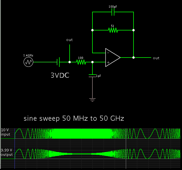
I have been told to study a design in which I have found an OP-Amp which I have been told to be working in non-inverting unity gain amplifier. But I can see that there is a 51 ohm resistor and 100pF capacitor connected in the feedback path.
Can anybody please tell me what might be the purpose of these two components in the feedback path of a unity gain amplifier. As far as I know there is no component in the feedback path of a unity gain amp. The ckt is attached herewith for reference.

Unity gain amp.jpg
 

This circuit isn't a unity gain amplifier , as per datashets.

It's clear that high frequency signal aren't welcomed, by the low pass on input, and also on the feed back.

The main reason I supose those unecessary components are there, is to void high frequency self oscilation, another things like that, at least for me is extremelly unusual yhose very small resistors values on Op circuitry, this means that they aren't usuless for things related to ofset stabilization.

If you simple CUT all 4 components, and conect directly the circuit will work for sure, but will not have a High Frequency filter included ( do not ask-me why )
 

The RC networks create a filter effect which lets through AC frequencies below 1.59 GHz. Frequencies above that are attenuated.

This is an unconventional design. I imagine this circuit is intended to make you think. Was it presented as a test question to troubleshoot?

Screenshot of my simulation:


The sine sweep is at 1.4 GHz. The output amplitude is starting to decline, as shown by the scope trace at extreme right.

The DC component is 5V. It is unchanged, being unity gain.
 

I have simulated the circuit and it confirms that the op-amp is in-fact used in unity gain configuration. The supply I used is 5V single supply (as in the original circuit) and supplied the input from 1.5V - 3.5V. I got exactly the same values at the output of op-amp. Any guesses?
I have further googled for this config and found some info that its related to cut-off frequencies. But since one LPF is already present at non-inv terminal why is the other in feedback path needed? Also, my input is pure dc.
 

I imagine this circuit is intended to make you think. Was it presented as a test question to troubleshoot?

Yes. I think so. Now I am have been given the same ckt with modified values as shown in below screenshot. I think the frequency calculations (1/2piRC) from the RC values gives the values of ~16MHz (input) and ~94.5MHz. Is it a band pass filter or band reject filter for AC frequencies or am I completely wrong here.
 

Attachments

  • Modified Values.JPG
    Modified Values.JPG
    34.8 KB · Views: 152
Last edited:

Real op amps are occasionally known to go into parasitic high-frequency oscillations (as Ebcir points out in post #2).
It is not always easy to figure out the root cause, or to find the direct cure.
Sometimes we have to try various cures, in one or more places.

This design has two RC networks which can reduce AC oscillations.
One is at the input, in case oscillations crop up there.
The other is in the feedback loop, in case they crop up there.

The simulator can not always reveal everything that might happen in real life. So when we apply DC, the simulation produces DC at unity gain... in agreement with simulated op amp rules of behavior.

I would imagine the professor is hoping you will test it with different waveforms, to find out when it is or is not unity gain.
Also, what must you do if you wish to reduce the rolloff frequency?
And why is there a difference between the RC time constant (a) at the input, and (b) in the feedback loop?
 

Now I am have been given the same ckt with modified values as shown in below screenshot. I think the frequency calculations (1/2piRC) from the RC values gives the values of ~16MHz (input) and ~94.5MHz. Is it a band pass filter or band reject filter for AC frequencies or am I completely wrong here.

I believe the action results in low pass, at a lower frequency than the first schematic.

To get an idea what kind of filter you have, try testing the response with only one capacitor connected.
Sweep a wide band to discover which part of the frequency spectrum is affected. You may have to sweep from 1 Hz to 100 GHz, to make sure.

Then repeat with only the other capacitor connected.

Then repeat with both capacitors.

That's the thorough, analytical method.
 

Long discussion about a silly schematic. All of the 4 components are simply meaningless for an OP with 5 MHz unity gain frequency. As far as shown it's just an unity gain amplifier, surrounded by some superfluous components.

The components might have an effect with high speed amplifiers. But I don't see a sense of discussing the said RC circuit without referring to specific OP parameters (what could be if...).
 
Status
Not open for further replies.

Part and Inventory Search

Welcome to EDABoard.com

Sponsor

Back
Top