Continue to Site

Welcome to EDAboard.com

Welcome to our site! EDAboard.com is an international Electronics Discussion Forum focused on EDA software, circuits, schematics, books, theory, papers, asic, pld, 8051, DSP, Network, RF, Analog Design, PCB, Service Manuals... and a whole lot more! To participate you need to register. Registration is free. Click here to register now.

Sroute on pads/nano route problem on soc encounter

Status
Not open for further replies.

conmourtz

Member level 1
Joined
Mar 29, 2012
Messages
36
Helped
0
Reputation
0
Reaction score
0
Trophy points
1,286
Location
Volos, Greece
Activity points
1,529
Hi there,

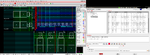
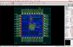
I have a design on Soc encounter. As you can see on the following attached files i have problem with pad vdd/vss power wiring on special route. i do the special route (i have 5 power signals for pads and 2 for core area). The 5th power siganl is only connected on the top of the design as you can see and on no other side of the design. Also, i tried put some more power pads on left, right and bottom and the same happened. No connection for the 5th power pad on left, right, bottom of the design. Secondly, when i do the nano route, the wires that connects the pads and the macro cells have some spacing problems as the violation report shows me. What could be wrong and how i can fix it? Please help me.

Best regards.
 

Attachments

  • Screenshot from 2013-02-23 21:58:08.png
    Screenshot from 2013-02-23 21:58:08.png
    175.2 KB · Views: 127
  • Screenshot from 2013-02-23 21:48:52.png
    Screenshot from 2013-02-23 21:48:52.png
    140.5 KB · Views: 120
Last edited:

The power pad ring should be made by the pad and the filler pad inside the row pad and also corner elements. Normally no special route should be added by the designer.
 

The power pad ring should be made by the pad and the filler pad inside the row pad and also corner elements. Normally no special route should be added by the designer.


i insert the pads on my design by modifying the netlist that design compiler exports. after that when i import the design on encounter i have to connect the power ring/stripes. the power pads connected with 5 power wires and the core design with 2 others. when i do the special route i choose all the power wires (7 total), and you see the connection it does on the attachment files. also i make the .ioc for the pads that shows the each pad location (corner,power or pad that transfers a signal on the core design). Is something wrong with my thoughts? If i do something wrong please tell me. Is there any other way to auto-import pads/power pads/filler pads on soc encounter? Thank you.
 

I dont understand why you need to add the pad in the netlist provided by DC.
The pads (digitals, not power pad) could be include in the RTL code, that better to control the correct functionality, and timing during DC.
In the PnR tool, you create the power nets, and you add the power pad with addInstance...
Do you need to create the 5 power wires which is only knowned by the power pad ring? I means the pad ring by itself will connect this 5 nets through the pads, the filler pads and the corner. The creation of this 5 power wires is only the cleanest way to generate a netlist with power net for LVS which will indcate the power connection of the power pad ring.

For the two core powers net, after the power creation, you need to connect the power pad which have a power-core pin to connect your internal ring to this pads.

Your design is pad limitd (means dependant of minimal bond pitch ?) or core limited.
If you have enoughe core space as you screen indicate, you could have all pads abuted, no space between them. Then no filler is needed.
 

i don't have an area specification for my design. You mean that i have to make a new toplevel on my design to connect the pads with the main design. Could you upload an example?

I attach the top level that i made and the warnings from dc


Do you see something wrong or how i can correct my warnings on dc?

Code:
check_design
Warning: In design 'slaveuniquify', input pin 'A' of leaf cell 'PAD_clk' is connected to undriven net 'clk'.  (LINT-58)
Warning: In design 'slaveuniquify', input pin 'A' of leaf cell 'PAD_reset' is connected to undriven net 'reset'.  (LINT-58)
Warning: In design 'slaveuniquify', input pin 'A' of leaf cell 'PAD_HSEL' is connected to undriven net 'HSEL'.  (LINT-58)
Warning: In design 'slaveuniquify', input pin 'A' of leaf cell 'PAD_HADDR3' is connected to undriven net 'HADDR[3]'.  (LINT-58)
Warning: In design 'slaveuniquify', input pin 'A' of leaf cell 'PAD_HADDR2' is connected to undriven net 'HADDR[2]'.  (LINT-58)
Warning: In design 'slaveuniquify', input pin 'A' of leaf cell 'PAD_HADDR1' is connected to undriven net 'HADDR[1]'.  (LINT-58)
Warning: In design 'slaveuniquify', input pin 'A' of leaf cell 'PAD_HWRITE' is connected to undriven net 'HWRITE'.  (LINT-58)
Warning: In design 'slaveuniquify', input pin 'A' of leaf cell 'PAD_HTRANS0' is connected to undriven net 'HTRANS[0]'.  (LINT-58)
Warning: In design 'slaveuniquify', input pin 'A' of leaf cell 'PAD_HTRANS1' is connected to undriven net 'HTRANS[1]'.  (LINT-58)
Warning: In design 'slaveuniquify', input pin 'A' of leaf cell 'PAD_HSIZE0' is connected to undriven net 'HSIZE[0]'.  (LINT-58)
Warning: In design 'slaveuniquify', input pin 'A' of leaf cell 'PAD_HSIZE1' is connected to undriven net 'HSIZE[1]'.  (LINT-58)
Warning: In design 'slaveuniquify', input pin 'A' of leaf cell 'PAD_HBURST0' is connected to undriven net 'HBURST[0]'.  (LINT-58)
Warning: In design 'slaveuniquify', input pin 'A' of leaf cell 'PAD_HBURST1' is connected to undriven net 'HBURST[1]'.  (LINT-58)
Warning: In design 'slaveuniquify', input pin 'A' of leaf cell 'PAD_HBURST2' is connected to undriven net 'HBURST[2]'.  (LINT-58)
Warning: In design 'slaveuniquify', input pin 'A' of leaf cell 'PAD_HADDR0' is connected to undriven net 'HADDR[0]'.  (LINT-58)
Warning: In design 'slaveuniquify', input pin 'A' of leaf cell 'PAD_HWDATA7' is connected to undriven net 'HWDATA[7]'.  (LINT-58)
Warning: In design 'slaveuniquify', input pin 'A' of leaf cell 'PAD_HWDATA6' is connected to undriven net 'HWDATA[6]'.  (LINT-58)
Warning: In design 'slaveuniquify', input pin 'A' of leaf cell 'PAD_HWDATA5' is connected to undriven net 'HWDATA[5]'.  (LINT-58)
Warning: In design 'slaveuniquify', input pin 'A' of leaf cell 'PAD_HWDATA4' is connected to undriven net 'HWDATA[4]'.  (LINT-58)
Warning: In design 'slaveuniquify', input pin 'A' of leaf cell 'PAD_HWDATA3' is connected to undriven net 'HWDATA[3]'.  (LINT-58)
Warning: In design 'slaveuniquify', input pin 'A' of leaf cell 'PAD_HWDATA2' is connected to undriven net 'HWDATA[2]'.  (LINT-58)
Warning: In design 'slaveuniquify', input pin 'A' of leaf cell 'PAD_HWDATA1' is connected to undriven net 'HWDATA[1]'.  (LINT-58)
Warning: In design 'slaveuniquify', input pin 'A' of leaf cell 'PAD_HWDATA0' is connected to undriven net 'HWDATA[0]'.  (LINT-58)
Warning: In design 'slaveuniquify', input pin 'A' of leaf cell 'PAD_STALL_PRE' is connected to undriven net 'STALL_pre'.  (LINT-58)
Warning: In design 'slaveuniquify', input port 'PI_clk' drives wired logic;
the port direction may have been specified incorrectly. (LINT-6)
Warning: In design 'slaveuniquify', input port 'PI_reset' drives wired logic;
the port direction may have been specified incorrectly. (LINT-6)
Warning: In design 'slaveuniquify', input port 'PI_HSEL' drives wired logic;
the port direction may have been specified incorrectly. (LINT-6)
Warning: In design 'slaveuniquify', input port 'PI_HADDR[3]' drives wired logic;
the port direction may have been specified incorrectly. (LINT-6)
Warning: In design 'slaveuniquify', input port 'PI_HADDR[2]' drives wired logic;
the port direction may have been specified incorrectly. (LINT-6)
Warning: In design 'slaveuniquify', input port 'PI_HADDR[1]' drives wired logic;
the port direction may have been specified incorrectly. (LINT-6)
Warning: In design 'slaveuniquify', input port 'PI_HADDR[0]' drives wired logic;
the port direction may have been specified incorrectly. (LINT-6)
Warning: In design 'slaveuniquify', input port 'PI_HBURST[2]' drives wired logic;
the port direction may have been specified incorrectly. (LINT-6)
Warning: In design 'slaveuniquify', input port 'PI_HBURST[1]' drives wired logic;
the port direction may have been specified incorrectly. (LINT-6)
Warning: In design 'slaveuniquify', input port 'PI_HBURST[0]' drives wired logic;
the port direction may have been specified incorrectly. (LINT-6)
Warning: In design 'slaveuniquify', input port 'PI_HSIZE[1]' drives wired logic;
the port direction may have been specified incorrectly. (LINT-6)
Warning: In design 'slaveuniquify', input port 'PI_HSIZE[0]' drives wired logic;
the port direction may have been specified incorrectly. (LINT-6)
Warning: In design 'slaveuniquify', input port 'PI_HTRANS[1]' drives wired logic;
the port direction may have been specified incorrectly. (LINT-6)
Warning: In design 'slaveuniquify', input port 'PI_HTRANS[0]' drives wired logic;
the port direction may have been specified incorrectly. (LINT-6)
Warning: In design 'slaveuniquify', input port 'PI_HWRITE' drives wired logic;
the port direction may have been specified incorrectly. (LINT-6)
Warning: In design 'slaveuniquify', input port 'PI_HWDATA[7]' drives wired logic;
the port direction may have been specified incorrectly. (LINT-6)
Warning: In design 'slaveuniquify', input port 'PI_HWDATA[6]' drives wired logic;
the port direction may have been specified incorrectly. (LINT-6)
Warning: In design 'slaveuniquify', input port 'PI_HWDATA[5]' drives wired logic;
the port direction may have been specified incorrectly. (LINT-6)
Warning: In design 'slaveuniquify', input port 'PI_HWDATA[4]' drives wired logic;
the port direction may have been specified incorrectly. (LINT-6)
Warning: In design 'slaveuniquify', input port 'PI_HWDATA[3]' drives wired logic;
the port direction may have been specified incorrectly. (LINT-6)
Warning: In design 'slaveuniquify', input port 'PI_HWDATA[2]' drives wired logic;
the port direction may have been specified incorrectly. (LINT-6)
Warning: In design 'slaveuniquify', input port 'PI_HWDATA[1]' drives wired logic;
the port direction may have been specified incorrectly. (LINT-6)
Warning: In design 'slaveuniquify', input port 'PI_HWDATA[0]' drives wired logic;
the port direction may have been specified incorrectly. (LINT-6)
Warning: In design 'slaveuniquify', input port 'PI_STALL_pre' drives wired logic;
the port direction may have been specified incorrectly. (LINT-6)
Warning: In design 'slaveuniquify', net 'HRDATA[0]' driven by pin 'PAD_HRDATA0/Y' has no loads. (LINT-2)
Warning: In design 'slaveuniquify', net 'HRDATA[1]' driven by pin 'PAD_HRDATA1/Y' has no loads. (LINT-2)
Warning: In design 'slaveuniquify', net 'HRDATA[2]' driven by pin 'PAD_HRDATA2/Y' has no loads. (LINT-2)
Warning: In design 'slaveuniquify', net 'HRDATA[3]' driven by pin 'PAD_HRDATA3/Y' has no loads. (LINT-2)
Warning: In design 'slaveuniquify', net 'HRDATA[4]' driven by pin 'PAD_HRDATA4/Y' has no loads. (LINT-2)
Warning: In design 'slaveuniquify', net 'HRDATA[5]' driven by pin 'PAD_HRDATA5/Y' has no loads. (LINT-2)
Warning: In design 'slaveuniquify', net 'HRDATA[6]' driven by pin 'PAD_HRDATA6/Y' has no loads. (LINT-2)
Warning: In design 'slaveuniquify', net 'HRDATA[7]' driven by pin 'PAD_HRDATA7/Y' has no loads. (LINT-2)
Warning: In design 'slaveuniquify', net 'HREADY' driven by pin 'PAD_HREADY/Y' has no loads. (LINT-2)
Warning: In design 'slaveuniquify', net 'HRESP' driven by pin 'PAD_HRESP/Y' has no loads. (LINT-2)
Warning: In design 'slaveuniquify', net 'STALL_pre' has no drivers.  Logic 0 assumed. (LINT-3)
Warning: In design 'slaveuniquify', net 'HWDATA[0]' has no drivers.  Logic 0 assumed. (LINT-3)
Warning: In design 'slaveuniquify', net 'HWDATA[1]' has no drivers.  Logic 0 assumed. (LINT-3)
Warning: In design 'slaveuniquify', net 'HWDATA[2]' has no drivers.  Logic 0 assumed. (LINT-3)
Warning: In design 'slaveuniquify', net 'HWDATA[3]' has no drivers.  Logic 0 assumed. (LINT-3)
Warning: In design 'slaveuniquify', net 'HWDATA[4]' has no drivers.  Logic 0 assumed. (LINT-3)
Warning: In design 'slaveuniquify', net 'HWDATA[5]' has no drivers.  Logic 0 assumed. (LINT-3)
Warning: In design 'slaveuniquify', net 'HWDATA[6]' has no drivers.  Logic 0 assumed. (LINT-3)
Warning: In design 'slaveuniquify', net 'HWDATA[7]' has no drivers.  Logic 0 assumed. (LINT-3)
Warning: In design 'slaveuniquify', net 'HBURST[0]' has no drivers.  Logic 0 assumed. (LINT-3)
Warning: In design 'slaveuniquify', net 'HBURST[1]' has no drivers.  Logic 0 assumed. (LINT-3)
Warning: In design 'slaveuniquify', net 'HBURST[2]' has no drivers.  Logic 0 assumed. (LINT-3)
Warning: In design 'slaveuniquify', net 'HSIZE[0]' has no drivers.  Logic 0 assumed. (LINT-3)
Warning: In design 'slaveuniquify', net 'HSIZE[1]' has no drivers.  Logic 0 assumed. (LINT-3)
Warning: In design 'slaveuniquify', net 'HTRANS[0]' has no drivers.  Logic 0 assumed. (LINT-3)
Warning: In design 'slaveuniquify', net 'HTRANS[1]' has no drivers.  Logic 0 assumed. (LINT-3)
Warning: In design 'slaveuniquify', net 'HWRITE' has no drivers.  Logic 0 assumed. (LINT-3)
Warning: In design 'slaveuniquify', net 'HADDR[0]' has no drivers.  Logic 0 assumed. (LINT-3)
Warning: In design 'slaveuniquify', net 'HADDR[1]' has no drivers.  Logic 0 assumed. (LINT-3)
Warning: In design 'slaveuniquify', net 'HADDR[2]' has no drivers.  Logic 0 assumed. (LINT-3)
Warning: In design 'slaveuniquify', net 'HADDR[3]' has no drivers.  Logic 0 assumed. (LINT-3)
Warning: In design 'slaveuniquify', net 'HSEL' has no drivers.  Logic 0 assumed. (LINT-3)
Warning: In design 'slaveuniquify', net 'reset' has no drivers.  Logic 0 assumed. (LINT-3)
Warning: In design 'slaveuniquify', net 'clk' has no drivers.  Logic 0 assumed. (LINT-3)
Information: In design 'slaveuniquify', net 'PI_STALL_pre' has multiple drivers.  Wired AND assumed. (LINT-4)
Information: In design 'slaveuniquify', net 'PI_HWDATA[0]' has multiple drivers.  Wired AND assumed. (LINT-4)
Information: In design 'slaveuniquify', net 'PI_HWDATA[1]' has multiple drivers.  Wired AND assumed. (LINT-4)
Information: In design 'slaveuniquify', net 'PI_HWDATA[2]' has multiple drivers.  Wired AND assumed. (LINT-4)
Information: In design 'slaveuniquify', net 'PI_HWDATA[3]' has multiple drivers.  Wired AND assumed. (LINT-4)
Information: In design 'slaveuniquify', net 'PI_HWDATA[4]' has multiple drivers.  Wired AND assumed. (LINT-4)
Information: In design 'slaveuniquify', net 'PI_HWDATA[5]' has multiple drivers.  Wired AND assumed. (LINT-4)
Information: In design 'slaveuniquify', net 'PI_HWDATA[6]' has multiple drivers.  Wired AND assumed. (LINT-4)
Information: In design 'slaveuniquify', net 'PI_HWDATA[7]' has multiple drivers.  Wired AND assumed. (LINT-4)
Information: In design 'slaveuniquify', net 'PI_HWRITE' has multiple drivers.  Wired AND assumed. (LINT-4)
Information: In design 'slaveuniquify', net 'PI_HTRANS[0]' has multiple drivers.  Wired AND assumed. (LINT-4)
Information: In design 'slaveuniquify', net 'PI_HTRANS[1]' has multiple drivers.  Wired AND assumed. (LINT-4)
Information: In design 'slaveuniquify', net 'PI_HSIZE[0]' has multiple drivers.  Wired AND assumed. (LINT-4)
Information: In design 'slaveuniquify', net 'PI_HSIZE[1]' has multiple drivers.  Wired AND assumed. (LINT-4)
Information: In design 'slaveuniquify', net 'PI_HBURST[0]' has multiple drivers.  Wired AND assumed. (LINT-4)
Information: In design 'slaveuniquify', net 'PI_HBURST[1]' has multiple drivers.  Wired AND assumed. (LINT-4)
Information: In design 'slaveuniquify', net 'PI_HBURST[2]' has multiple drivers.  Wired AND assumed. (LINT-4)
Information: In design 'slaveuniquify', net 'PI_HADDR[0]' has multiple drivers.  Wired AND assumed. (LINT-4)
Information: In design 'slaveuniquify', net 'PI_HADDR[1]' has multiple drivers.  Wired AND assumed. (LINT-4)
Information: In design 'slaveuniquify', net 'PI_HADDR[2]' has multiple drivers.  Wired AND assumed. (LINT-4)
Information: In design 'slaveuniquify', net 'PI_HADDR[3]' has multiple drivers.  Wired AND assumed. (LINT-4)
Information: In design 'slaveuniquify', net 'PI_HSEL' has multiple drivers.  Wired AND assumed. (LINT-4)
Information: In design 'slaveuniquify', net 'PI_reset' has multiple drivers.  Wired AND assumed. (LINT-4)
Information: In design 'slaveuniquify', net 'PI_clk' has multiple drivers.  Wired AND assumed. (LINT-4)
Information: In design 'slaveuniquify', net 'ahb_slave/DIN[0]' has multiple drivers.  Wired AND assumed. (LINT-4)
Information: In design 'slaveuniquify', net 'ahb_slave/DIN[1]' has multiple drivers.  Wired AND assumed. (LINT-4)
Information: In design 'slaveuniquify', net 'ahb_slave/DIN[2]' has multiple drivers.  Wired AND assumed. (LINT-4)
Information: In design 'slaveuniquify', net 'ahb_slave/DIN[3]' has multiple drivers.  Wired AND assumed. (LINT-4)
Information: In design 'slaveuniquify', net 'ahb_slave/DIN[4]' has multiple drivers.  Wired AND assumed. (LINT-4)
Information: In design 'slaveuniquify', net 'ahb_slave/DIN[5]' has multiple drivers.  Wired AND assumed. (LINT-4)
Information: In design 'slaveuniquify', net 'ahb_slave/DIN[6]' has multiple drivers.  Wired AND assumed. (LINT-4)
Information: In design 'slaveuniquify', net 'ahb_slave/DIN[7]' has multiple drivers.  Wired AND assumed. (LINT-4)
Warning: In design 'ahb_slave_ram', port 'HBURST[2]' is not connected to any nets. (LINT-28)
Warning: In design 'ahb_slave_ram', port 'HBURST[1]' is not connected to any nets. (LINT-28)
Warning: In design 'ahb_slave_ram', port 'HBURST[0]' is not connected to any nets. (LINT-28)
Warning: In design 'ahb_slave_ram', port 'HSIZE[1]' is not connected to any nets. (LINT-28)
Warning: In design 'ahb_slave_ram', port 'HSIZE[0]' is not connected to any nets. (LINT-28)
Warning: In design 'ahb_slave_ram', input port 'HWDATA[7]' is connected directly to output port 'DIN[7]'. (LINT-29)
Warning: In design 'ahb_slave_ram', input port 'HWDATA[6]' is connected directly to output port 'DIN[6]'. (LINT-29)
Warning: In design 'ahb_slave_ram', input port 'HWDATA[5]' is connected directly to output port 'DIN[5]'. (LINT-29)
Warning: In design 'ahb_slave_ram', input port 'HWDATA[4]' is connected directly to output port 'DIN[4]'. (LINT-29)
Warning: In design 'ahb_slave_ram', input port 'HWDATA[3]' is connected directly to output port 'DIN[3]'. (LINT-29)
Warning: In design 'ahb_slave_ram', input port 'HWDATA[2]' is connected directly to output port 'DIN[2]'. (LINT-29)
Warning: In design 'ahb_slave_ram', input port 'HWDATA[1]' is connected directly to output port 'DIN[1]'. (LINT-29)
Warning: In design 'ahb_slave_ram', input port 'HWDATA[0]' is connected directly to output port 'DIN[0]'. (LINT-29)


Code:
module slaveuniquify (
	PI_clk, 
	PI_reset, 
	PI_HSEL, 
	PI_HADDR, 
	PI_HBURST, 
	PI_HSIZE, 
	PI_HTRANS, 
	PI_HWRITE, 
	PI_HWDATA, 
	PO_HRDATA, 
	PO_HREADY, 
	PO_HRESP, 
	PI_STALL_pre);

   input PI_clk;
   input PI_reset;
   input PI_HSEL;
   input [3:0] PI_HADDR;
   input [2:0] PI_HBURST;
   input [1:0] PI_HSIZE;
   input [1:0] PI_HTRANS;
   input PI_HWRITE;
   input [7:0] PI_HWDATA;
   output [7:0] PO_HRDATA;
   output PO_HREADY;
   output PO_HRESP;
   input PI_STALL_pre;
   
   
   wire clk;
   wire reset;
   wire HSEL;
   wire [3:0] HADDR;
   wire [2:0] HBURST;
   wire [1:0] HSIZE;
   wire [1:0] HTRANS;
   wire HWRITE;
   wire [7:0] HWDATA;
   wire [7:0] HRDATA;
   wire HREADY;
   wire HRESP;
   wire STALL_pre;


   ahb_slave ahb_slave ( .clk(PI_clk),
								 .reset(PI_reset),
								 .HSEL(PI_HSEL),
								 .HADDR(PI_HADDR),
								 .HBURST(PI_HBURST),
								 .HSIZE(PI_HSIZE),
								 .HTRANS(PI_HTRANS),
								 .HWRITE(PI_HWRITE),
								 .HWDATA(PI_HWDATA),
								 .HRDATA(PO_HRDATA),
								 .HREADY(PO_HREADY),
								 .HRESP(PO_HRESP),
								 .STALL_pre(PI_STALL_pre)
				 );


   //Input pads
   
   
   //clk, reset pads N pads
   
   BUDU12P_V5 PAD_clk (.PAD(PI_clk), .A(clk));
   
   BUDU12P_V5 PAD_reset (.PAD(PI_reset), .A(reset));
   
   BUDU12P_V5 PAD_HSEL (.PAD(PI_HSEL), .A(HSEL));
   
   BUDU12P_V5 PAD_HADDR3 (.PAD(PI_HADDR[3]),
					  .A(HADDR[3]));
   BUDU12P_V5 PAD_HADDR2 (.PAD(PI_HADDR[2]),
					  .A(HADDR[2]));
   BUDU12P_V5 PAD_HADDR1 (.PAD(PI_HADDR[1]),
					  .A(HADDR[1]));
   
   
   //W pads
   
   BUDU12P_V5 PAD_HWRITE (.PAD(PI_HWRITE),
					  .A(HWRITE));
   
   BUDU12P_V5 PAD_HTRANS0 (.PAD(PI_HTRANS[0]),
					   .A(HTRANS[0]));
   BUDU12P_V5 PAD_HTRANS1 (.PAD(PI_HTRANS[1]),
					   .A(HTRANS[1]));
   
   BUDU12P_V5 PAD_HSIZE0 (.PAD(PI_HSIZE[0]),
					  .A(HSIZE[0]));
   BUDU12P_V5 PAD_HSIZE1 (.PAD(PI_HSIZE[1]),
					  .A(HSIZE[1]));
   
   BUDU12P_V5 PAD_HBURST0 (.PAD(PI_HBURST[0]),
					   .A(HBURST[0]));
   BUDU12P_V5 PAD_HBURST1 (.PAD(PI_HBURST[1]),
					   .A(HBURST[1]));
   BUDU12P_V5 PAD_HBURST2 (.PAD(PI_HBURST[2]),
					   .A(HBURST[2]));
   
   BUDU12P_V5 PAD_HADDR0 (.PAD(PI_HADDR[0]),
					  .A(HADDR[0]));
   
   //S pads
   
   BUDU12P_V5 PAD_HWDATA7 (.PAD(PI_HWDATA[7]),
					   .A(HWDATA[7]));
   BUDU12P_V5 PAD_HWDATA6 (.PAD(PI_HWDATA[6]),
					   .A(HWDATA[6]));
   BUDU12P_V5 PAD_HWDATA5 (.PAD(PI_HWDATA[5]),
					   .A(HWDATA[5]));
   BUDU12P_V5 PAD_HWDATA4 (.PAD(PI_HWDATA[4]),
					   .A(HWDATA[4]));
   BUDU12P_V5 PAD_HWDATA3 (.PAD(PI_HWDATA[3]),
					   .A(HWDATA[3]));
   BUDU12P_V5 PAD_HWDATA2 (.PAD(PI_HWDATA[2]),
					   .A(HWDATA[2]));
   BUDU12P_V5 PAD_HWDATA1 (.PAD(PI_HWDATA[1]),
					   .A(HWDATA[1]));
   BUDU12P_V5 PAD_HWDATA0 (.PAD(PI_HWDATA[0]),
					   .A(HWDATA[0]));
   
   
   //E pads
   
   BUDU12P_V5 PAD_STALL_PRE (.PAD(PI_STALL_pre),
						 .A(STALL_pre));


   //Output pads
   
   //S pads
   
   //E pads
   
   ITUP_V5 PAD_HRESP (.PAD(PO_HRESP),
					   .Y(HRESP));
   
   ITUP_V5 PAD_HREADY (.PAD(PO_HREADY),
						.Y(HREADY));
   
   
   ITUP_V5 PAD_HRDATA0 (.PAD(PO_HRDATA[0]),
						 .Y(HRDATA[0]));
   ITUP_V5 PAD_HRDATA1 (.PAD(PO_HRDATA[1]),
						 .Y(HRDATA[1]));
   ITUP_V5 PAD_HRDATA2 (.PAD(PO_HRDATA[2]),
						 .Y(HRDATA[2]));
   ITUP_V5 PAD_HRDATA3 (.PAD(PO_HRDATA[3]),
						 .Y(HRDATA[3]));
   ITUP_V5 PAD_HRDATA4 (.PAD(PO_HRDATA[4]),
						 .Y(HRDATA[4]));
   ITUP_V5 PAD_HRDATA5 (.PAD(PO_HRDATA[5]),
						 .Y(HRDATA[5]));
   ITUP_V5 PAD_HRDATA6 (.PAD(PO_HRDATA[6]),
						 .Y(HRDATA[6]));
   ITUP_V5 PAD_HRDATA7 (.PAD(PO_HRDATA[7]),
						 .Y(HRDATA[7]));


   //vdd-vss
   
    //VDD: VDD5RP_V5;
    //VSS: GND5RP_V5;


   endmodule
 
Last edited:

well, to the module ahb_slave you should connect the core-pin side of the pad, not the pad side, like for PI_clk goes to pin PAD of your input-pad component and the output pin (core side) connected to net "clk" should be used to your ahb_slave module, seem all yours pads is not correctly connected.
Did you re-run your regression tests suit?
 
I changed the RTL on my design. Now pads are correctly connected (as far as i can see on encounter and no warnings/errors on DC). The power wires are all connected on pads, but they have still the short violation problem. Also some wires from pads (as you can see on my initial post attachments) that lead to a macro cell on my design have short violations. what could be wrong?
 

Where comes from the METAL3 ring over the pads?
 

the ring over pads which is on metal 3 is when i special route the design. i select all the power nets (5 of pads + 2 of core) and the tool automatically connects the power ring over the pads. What can i do for that? To avoid these short violations for the power ring on pads?
 

if your pad ring is full with pads and corner you do not need to route these 5 net that are only in the pad ring, in all case the power pad ring will be route with the pad and the pad filler.
 

if i don't include these power wires on the

Code:
Power -> Connect Global Nets


option on Soc encounter when i check the power it shows me warning for these pads that are not connected. So, i connect them all with

Code:
globalNetConnect vdd! -type pgpin -pin vdd! -inst * -verbose
globalNetConnect gnd! -type pgpin -pin gnd! -inst * -verbose
globalNetConnect gnd5o! -type pgpin -pin gnd5o! -inst * -verbose
globalNetConnect gnd5r! -type pgpin -pin gnd5r! -inst * -verbose
globalNetConnect vdd3r! -type pgpin -pin vdd3r! -inst * -verbose
globalNetConnect vdd5o! -type pgpin -pin vdd5o! -inst * -verbose
globalNetConnect vdd5r! -type pgpin -pin vdd5r! -inst * -verbose
globalNetConnect vdd! -type pgpin -pin A -sinst PAD_VDD -verbose
globalNetConnect gnd! -type pgpin -pin A -sinst PAD_VSS -verbose


and then i create core ring and stripes.

on
Code:
Route->special route

i select all the power wires and **** the options checked on Sroute that follows then i click ok and soce connects these power wires with all pads and the wires vdd! and gnd! on the rows on the core design.

When i after run verify geometry i have all these ghort violation problem. So the bottom line is that these wires have to be connected with the pads. Why i get the short violation?
 

Well,
1- first the pairing need to be full with pads, corners, pad fillers.
2-Then with globalist connect, you made the logical connection to have the netlist properly generated with the power nets.
3-with sroute, you only route the two core power nets.
4-during the final LVS the tool could mention that the power pad nets is unconnected but you could ignore this 5 warning and the layout and the netlist will be clean.
 
Status
Not open for further replies.

Part and Inventory Search

Welcome to EDABoard.com

Sponsor

Back
Top