mehra_pallavi
Newbie level 4
Would appreciate any kind of help with the Verilog project I'm trying to complete.
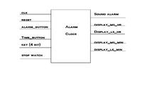
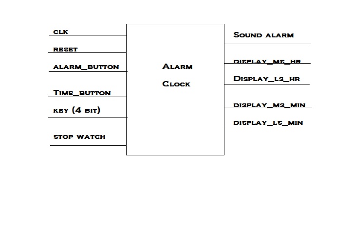
Description: Its a digital alarm clock that displays time in the LCD display format. The final output should be programmed onto a spartan 3 FPGA board.
I/O Ports:
1.) "clk"is a 256Hz clock
2.)"reset" is an asynchronous active high
3.)Key is the 4 bit key input
4.) "alarm_button" is an active high control signal for setting alarm time
5.) "time_button" is an active control signal for setting current time
6.) "sound_alarm" is an active high output
7.) "Display Time" are the outputs which display the values in LCD format
8.) "stop_watch" mode
IMAGE FOR BLOCK DIAGRAM ATTACHED
This top module has six-sub modules
a.) Time generator
b.) Key Register
c.) Alarm Register
d.) Counter
e.) Alarm Controller
f.) Display Driver
ANY help would be greatly appreciated. Thank You