Vermes
Advanced Member level 4
Sometimes you need to make a PCB in short time, you may also need to create prototypes or your PCB requires changes. Then, when there is no time for order in professionals, you may need an alternative which is quicker and cheaper, although still of good quality. Thermal transfer method seems to be perfect, but it is not always repeatable. So, you can use the photochemical method. The process of performing boards in this method involves exposure of lacquer/photosensitive film with ultraviolet rays. Such a device for UV exposure can be performed at an electronic workshop and this article shows the construction.
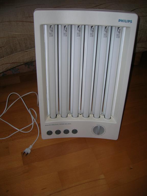
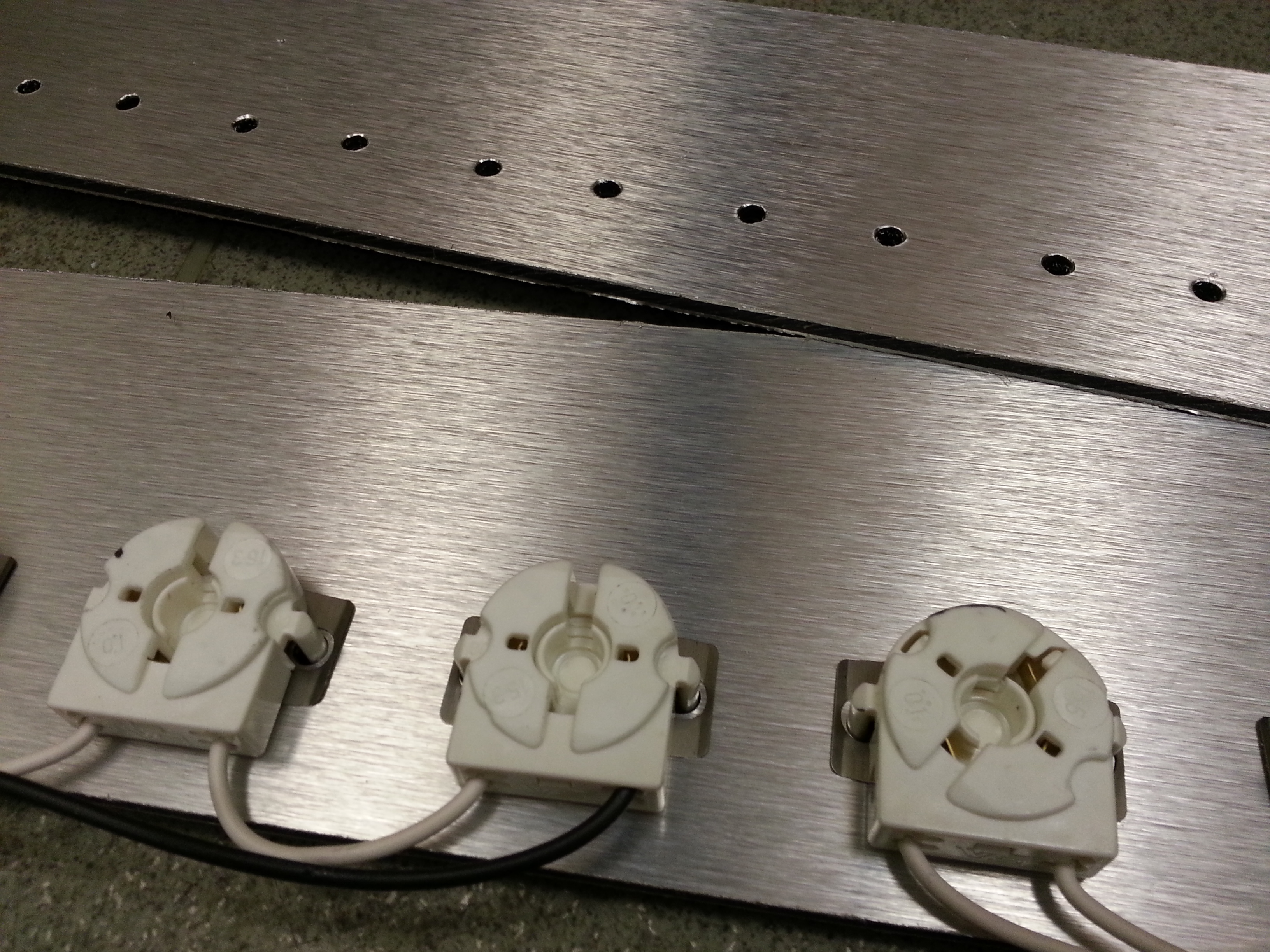
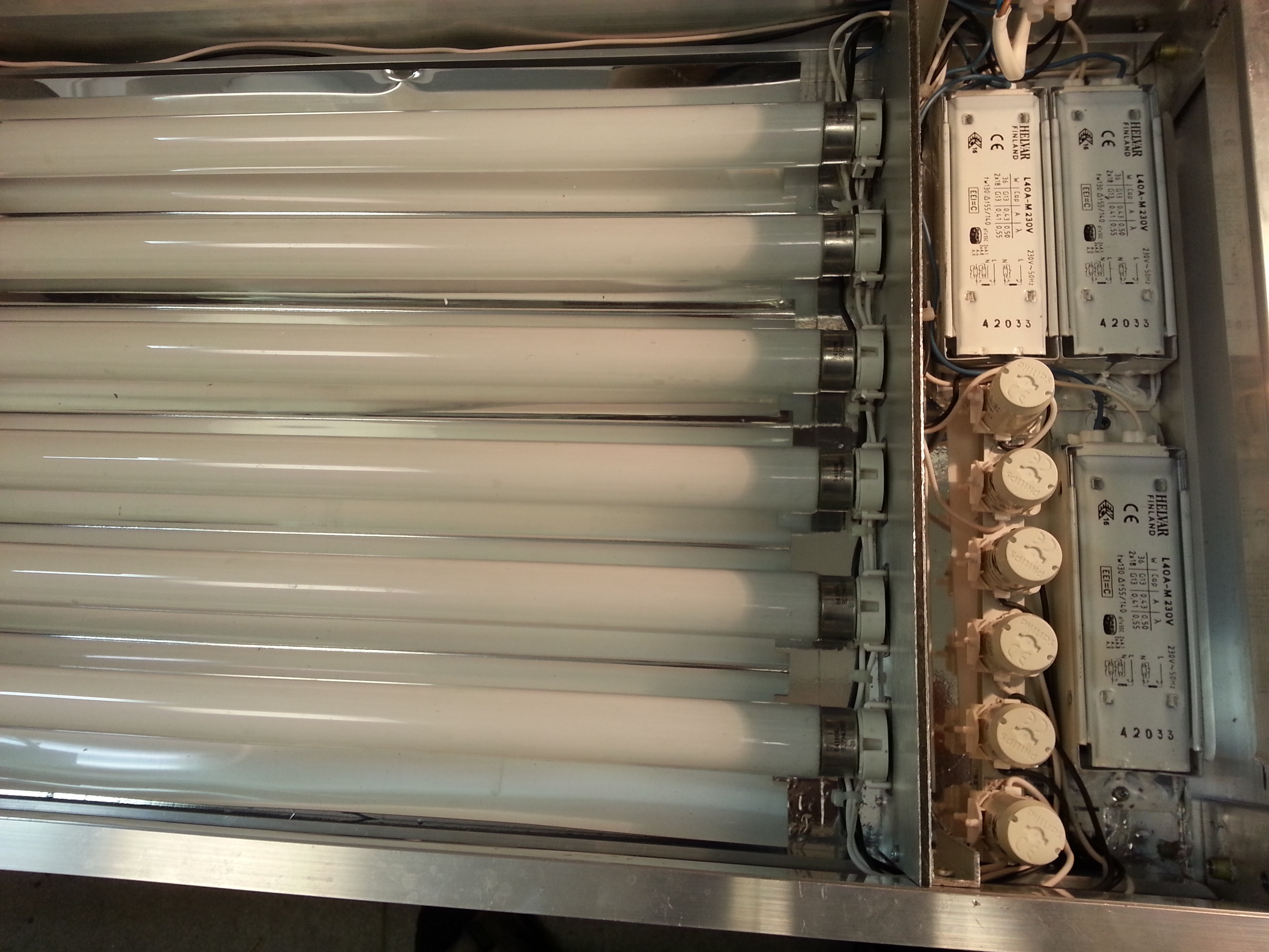
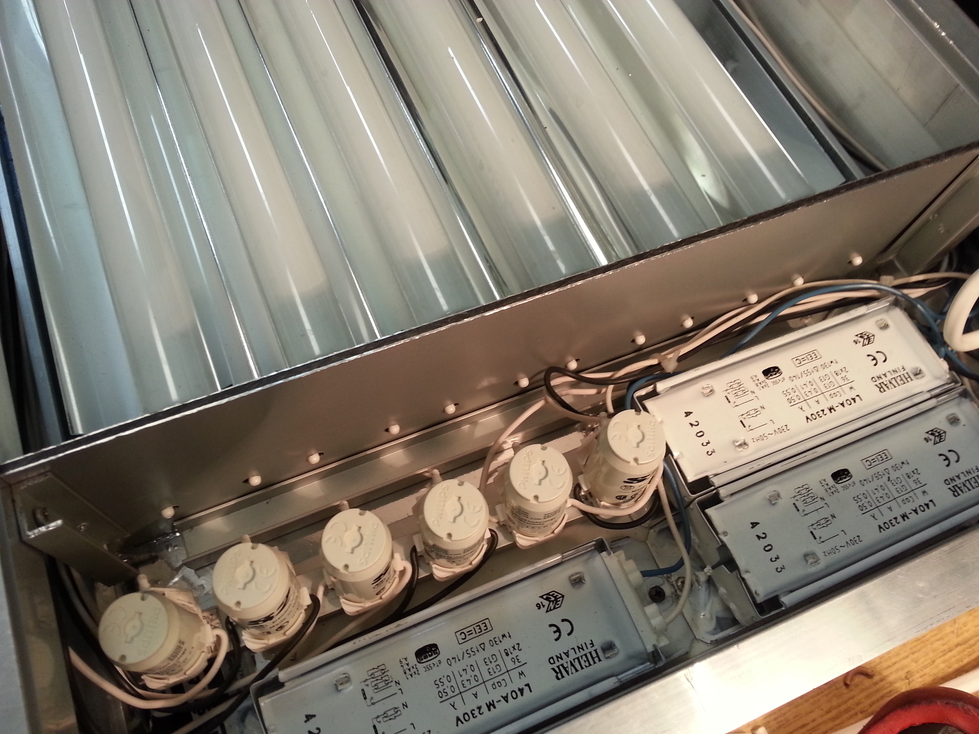
For your design you will need a portable solarium, which can be easily purchased in an auction portal. This device uses Philips solarium with six fluorescent lights 20W.
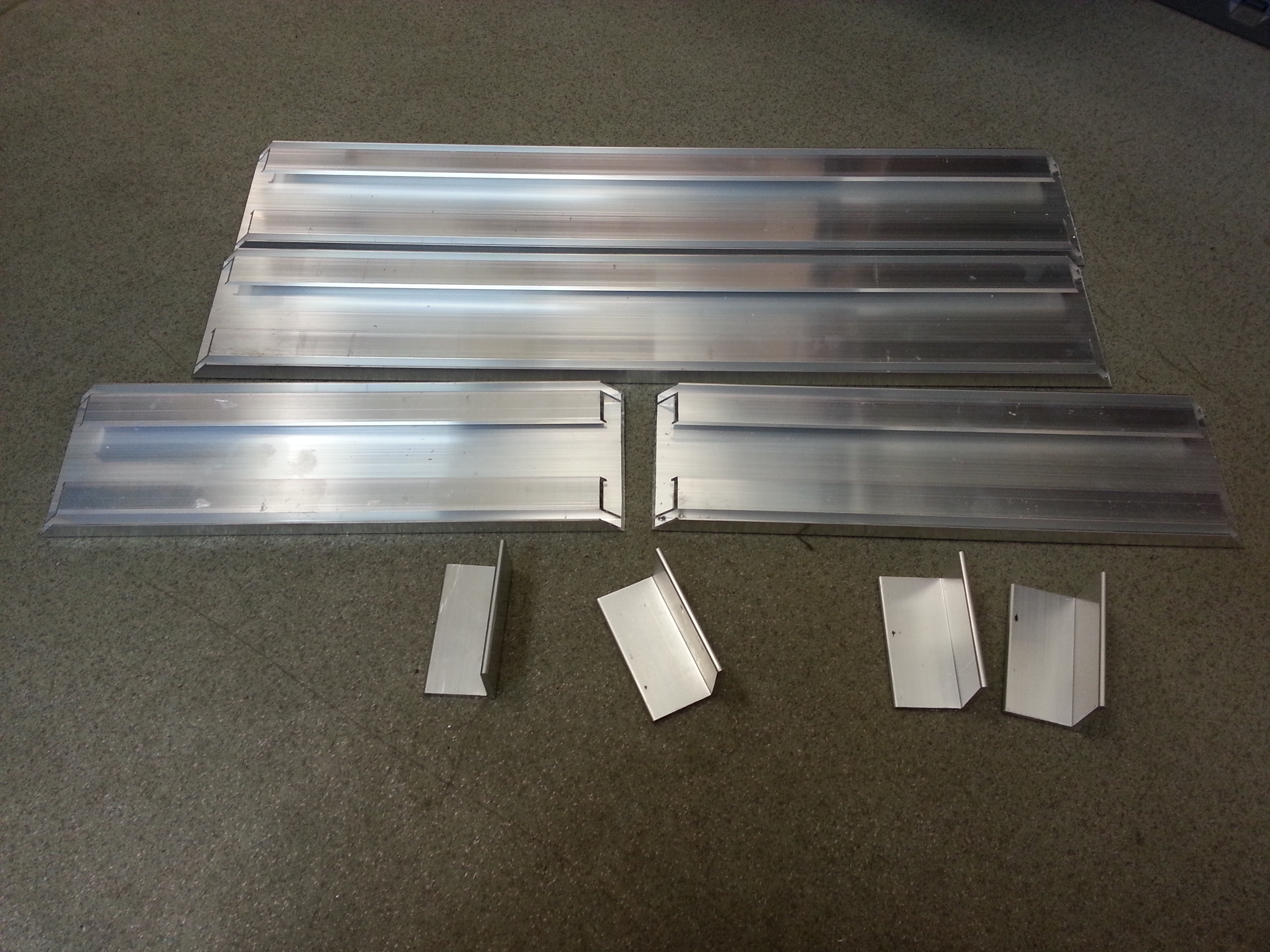
The construction also uses four aluminum profiles, four angles, PVC foam board, two plates of dibond and 5mm thick glass.
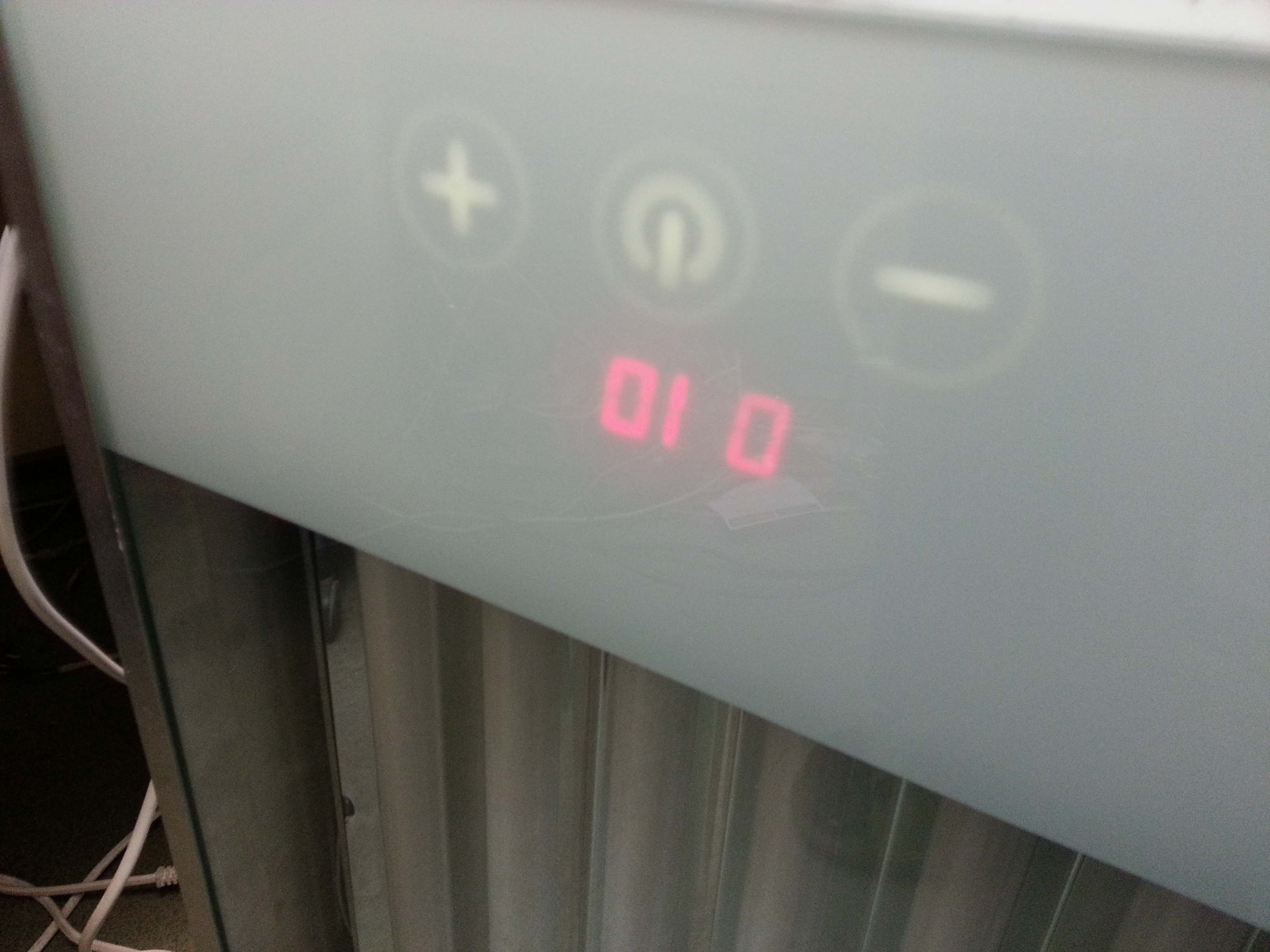
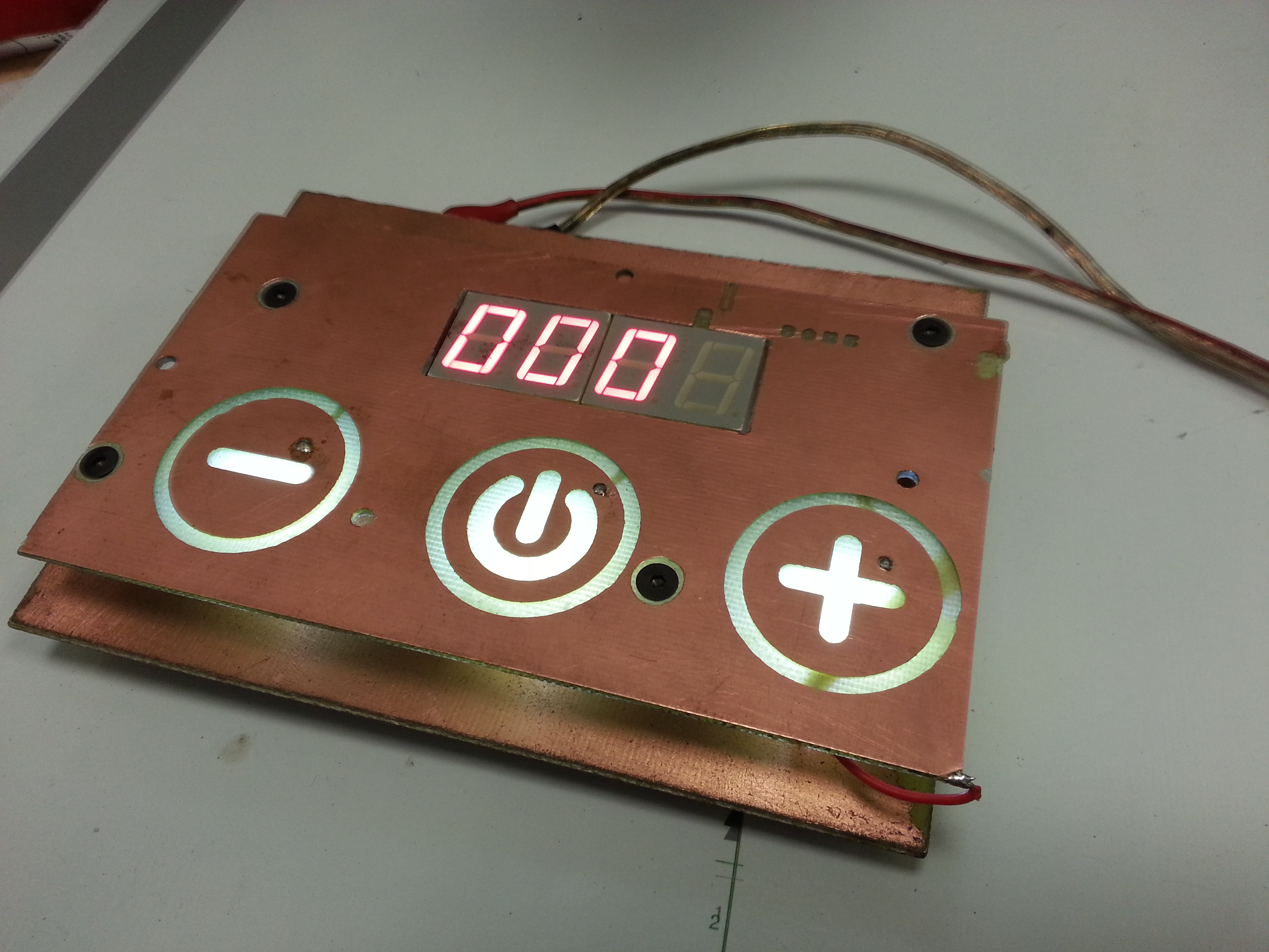
The main electronic component is Atmega8A. Time is displayed on standard LED displays. Touch control is based on AT42QT1010-TSHR.
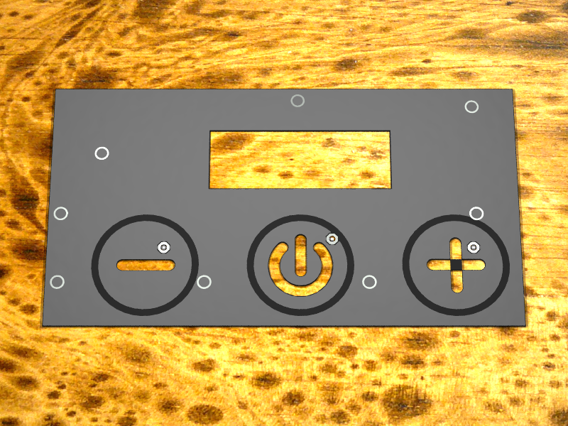
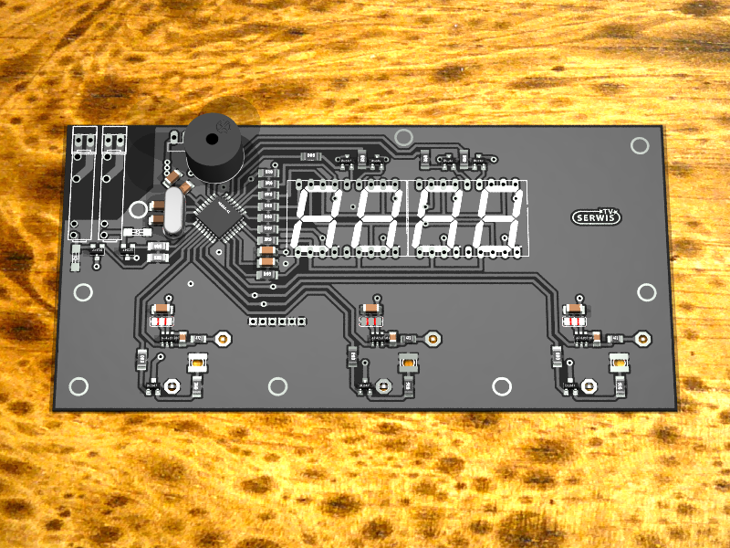

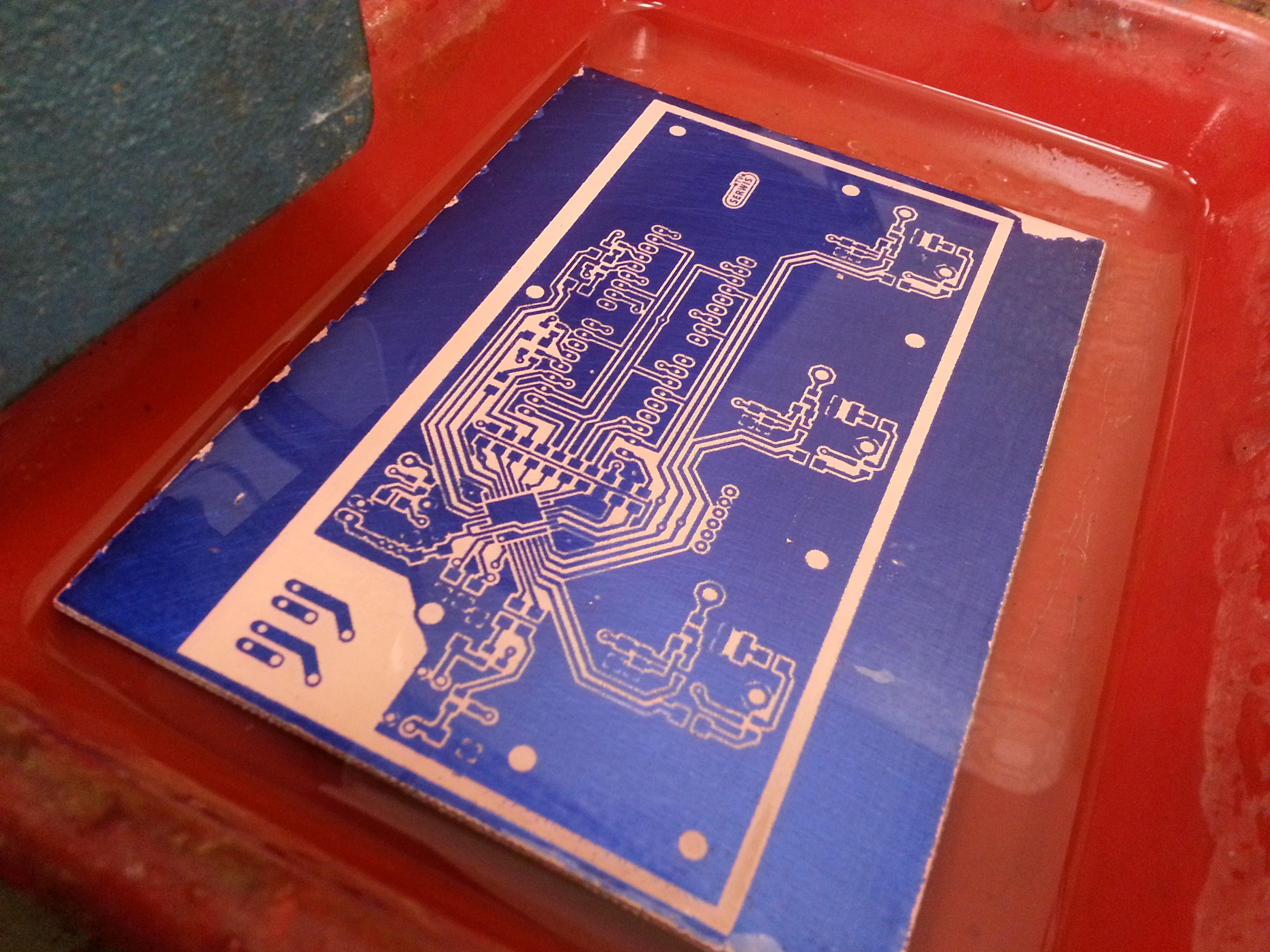
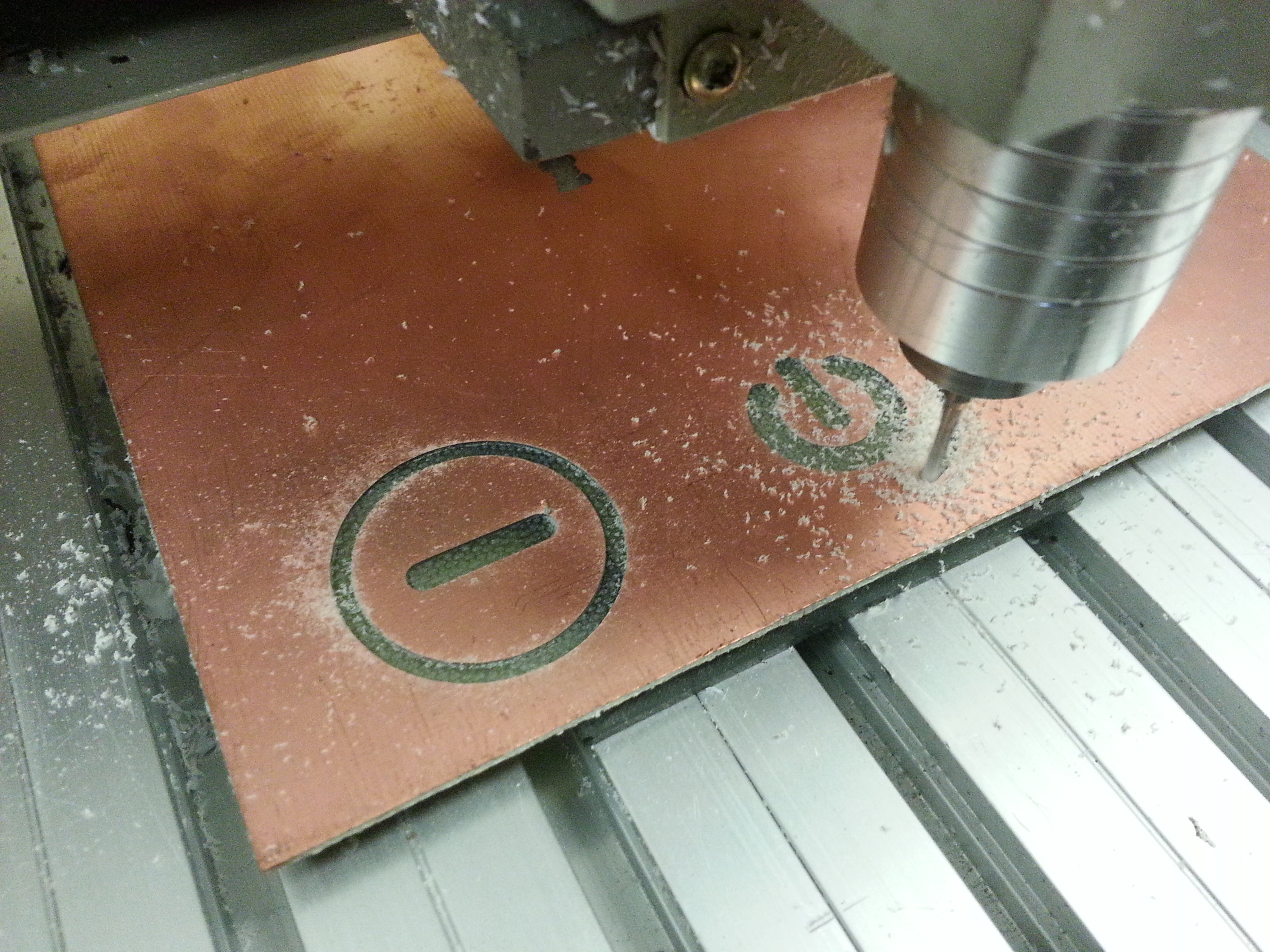
The bottom PCB was made in photochemical method, the upper PCB with buttons was made on a CNC machine. That allows the light of LEDs to pass through the board.
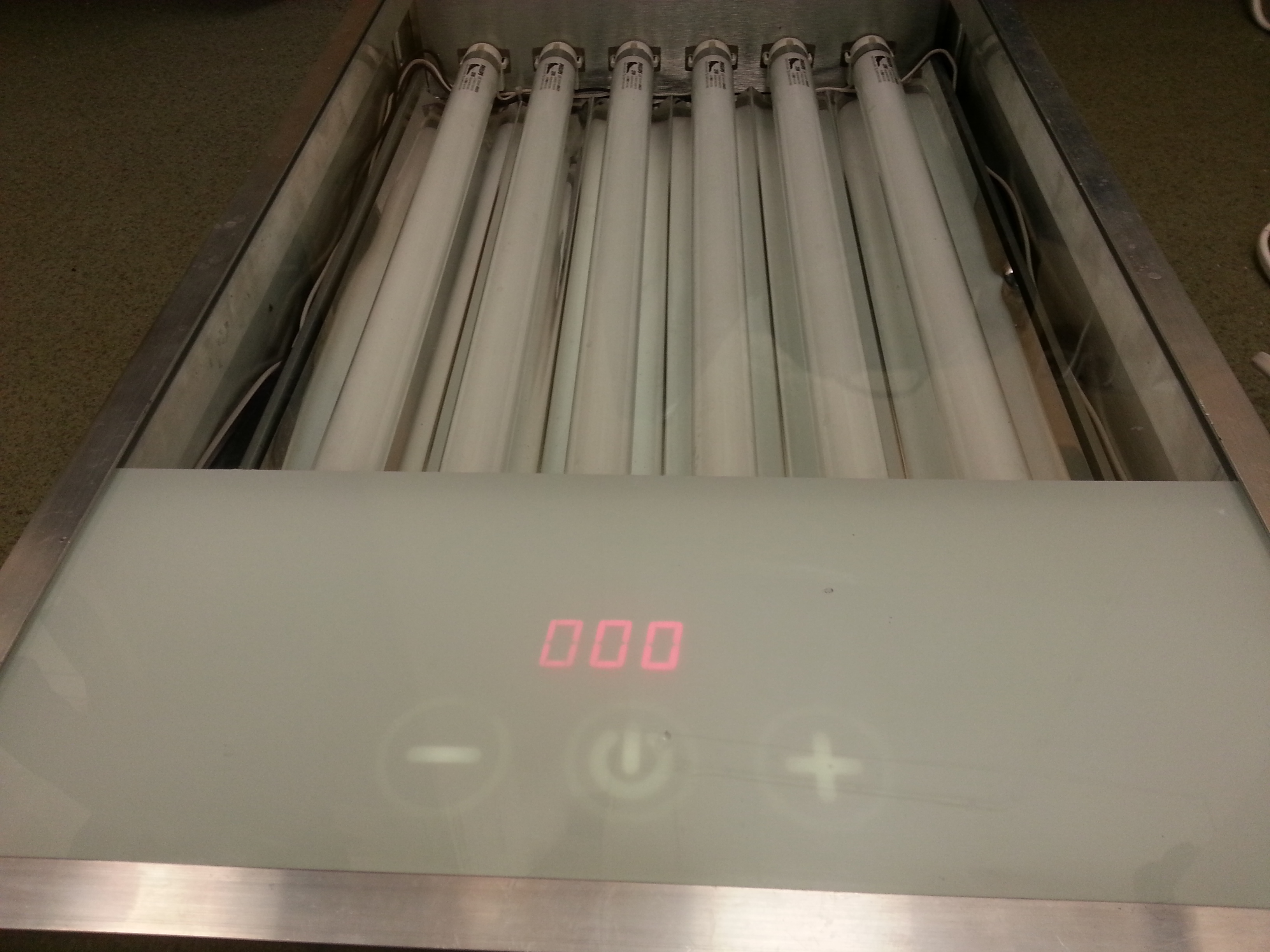
Then glass was painted white.
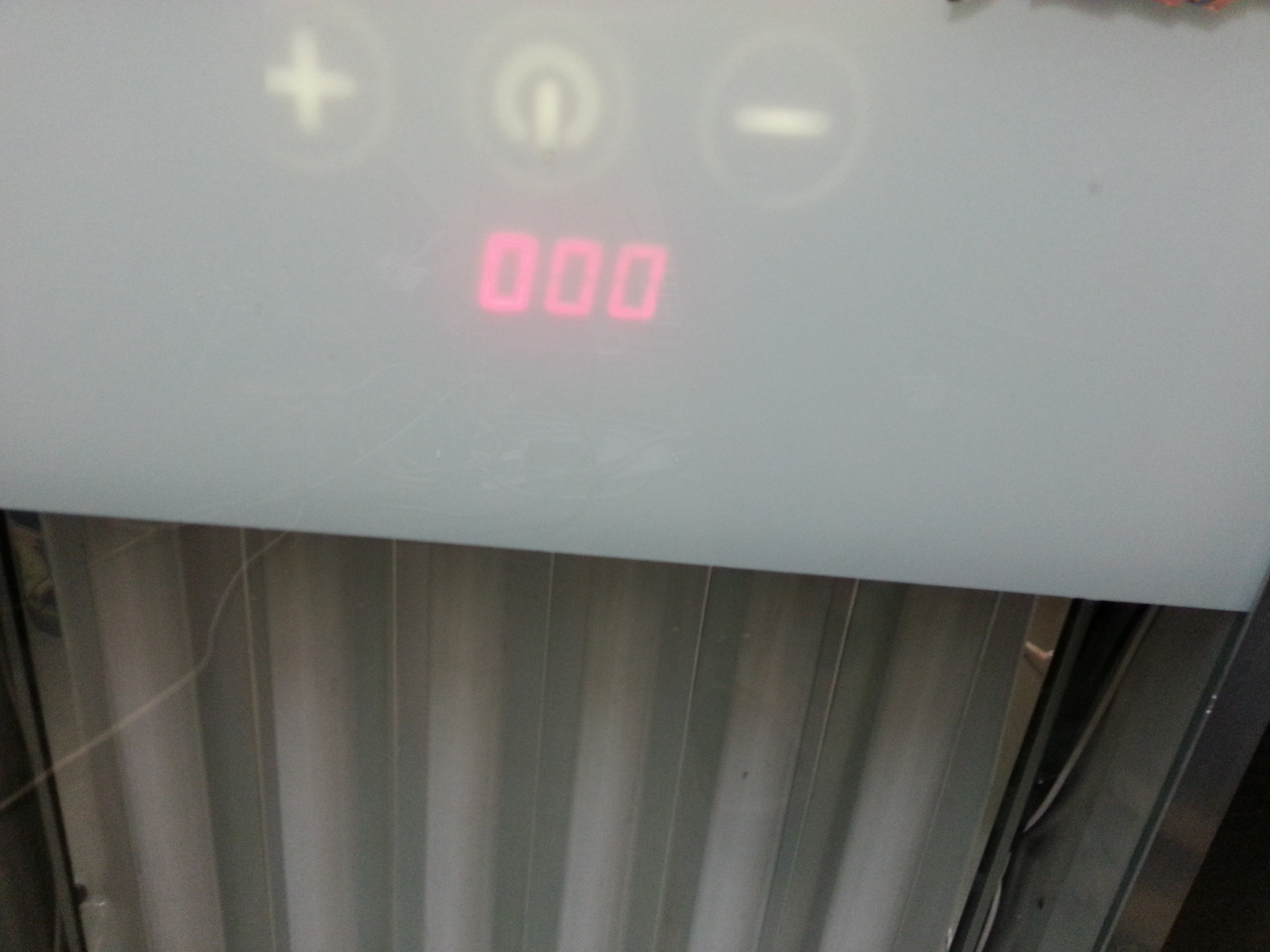
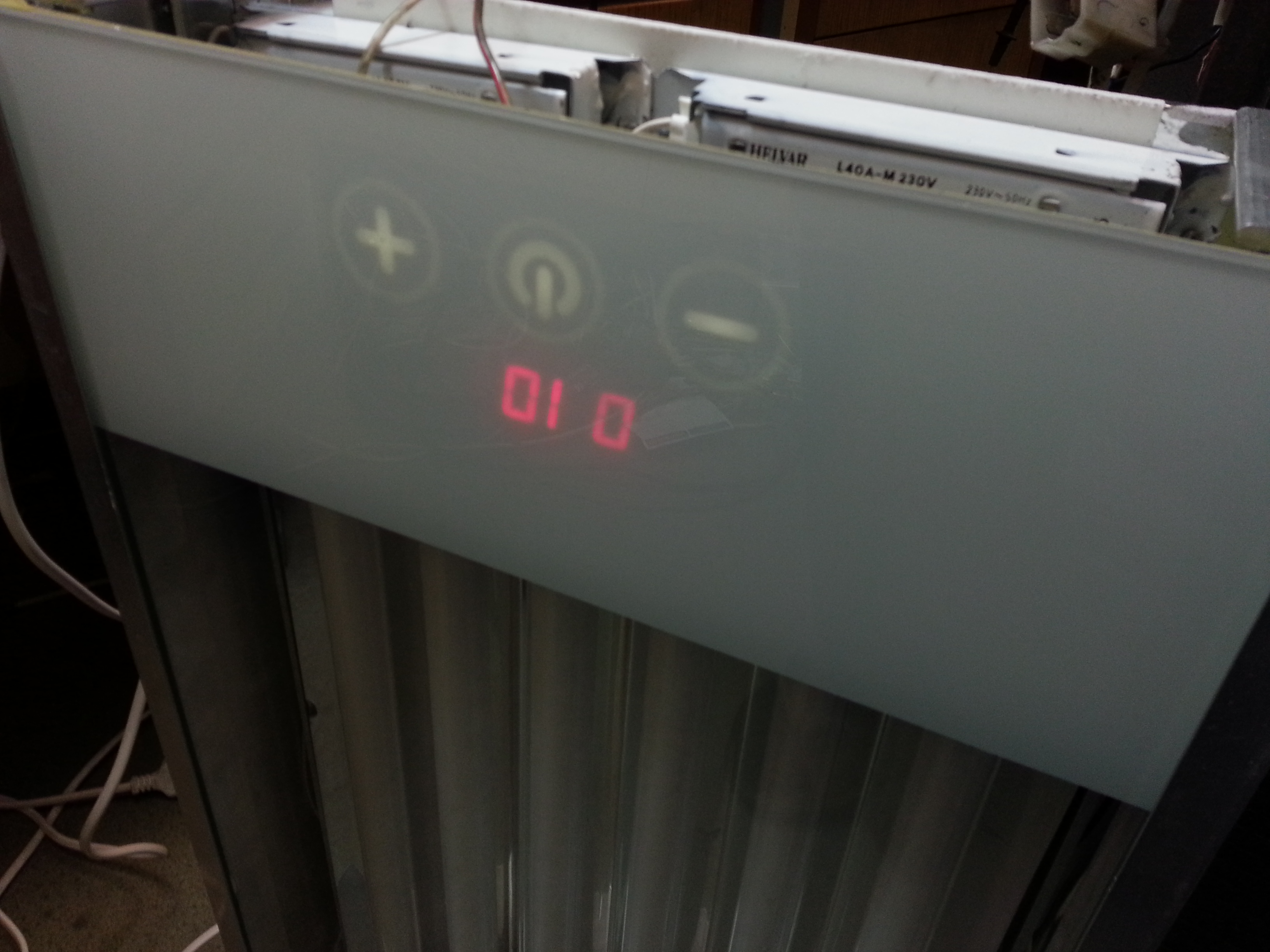
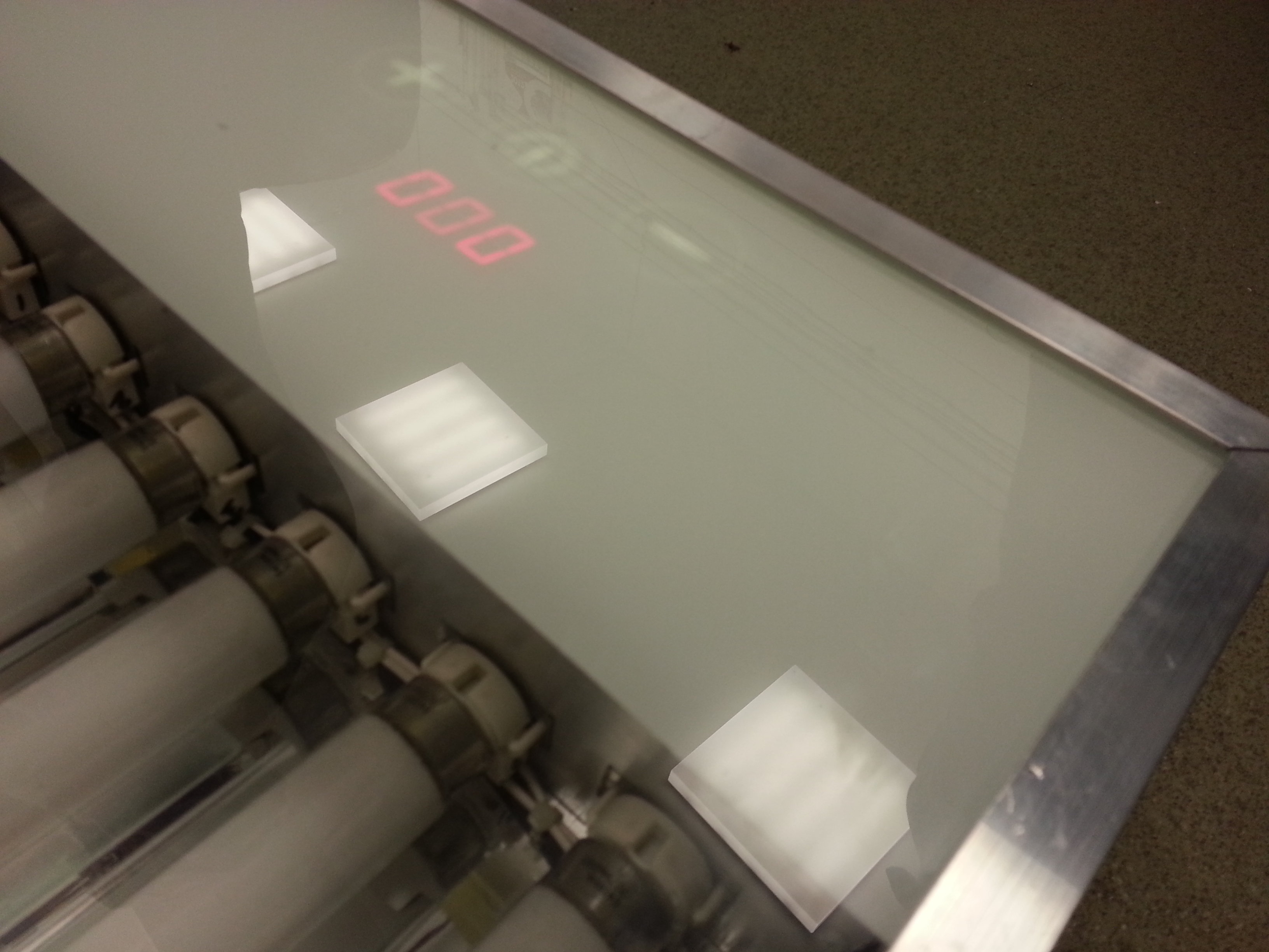
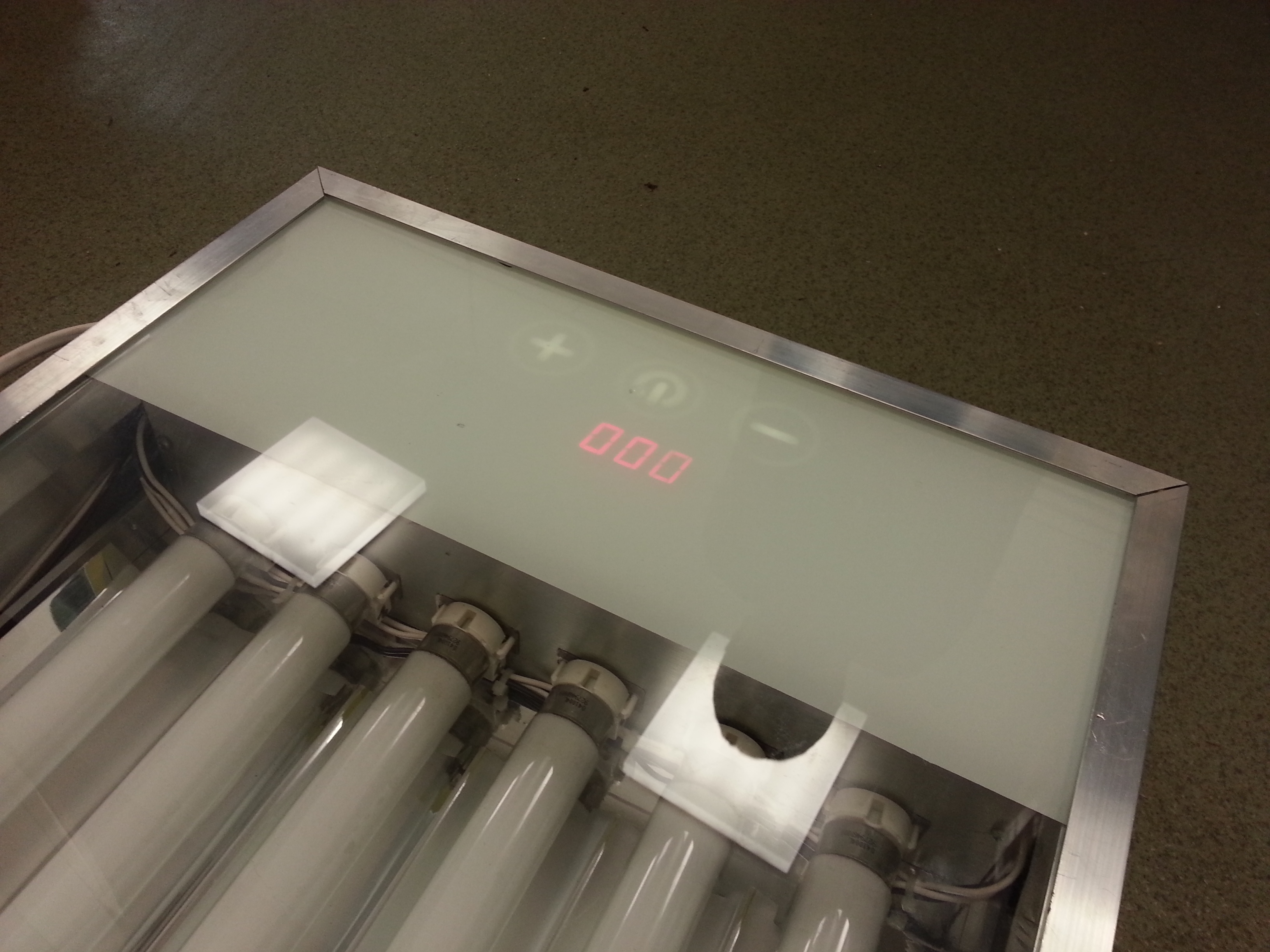
There are three buttons for the control. Buttons + and ? Are for setting the time of exposure, and the central button is for switching on and off the device when the time is not passed yet.
The design can be modified so that the device switches on only after closing the upper lid of dibond. The touchpads are so sensitive that they perfectly detect the presence of dibond.
Optimal time of exposure of a PCB is 45 seconds.
List of elements used:
- solarium
- profile
- small boards of dibond
- large board of dibond
- 5mm thick glass
- Atmega8
- AT42QT1010-TSHR
- LED display
- LED
- relay
Pictures of the construction:

And a video (more videos can be found on the original thread - link below):
Link to original thread (useful attachment) - Naświetlarka UV do płytek PCB z touch sensorem