forgoreth
Newbie level 6
Hello everyone,
I was going to build a buck converter today but -knowing the difficulties of high-side driving- I thought it is better to just drive the MOSFET in the low-side with just a resistive load for exercise. But I failed...
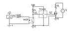
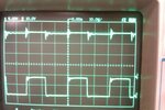
I am producing my PWM signal by an Arduino microcontroller and the duty cycle can be adjusted by a potentiometer. PWM signal goes to the MOSFET gate via an opto-isolator and a MOSFET driver. Everything about the gate signal looks fine. But unfortunately, MOSFET did not turn "off". After I took the photo, I connected a RCD snubber between the source and the drain but it did not affect at all (maybe because I don't know how to design a proper snubber. R=150 Ohms, C=10nF and the diode is 1N4148); I am attaching my circuit schematic, my gate signal and the voltage on the load oscilloscope screens. I used IXKP20N MOSFET; Vdd is 15V; Vi is 20V and Rload is a variable resistor. The current was between 500mA-1A.
I have three questions:
1-) What may be the reason for staying in "on" state?
2-) 4n25 optoisolator has bad rise and fall times and this leads to phase shift between generated PWM and gate signal. This can be tolerated but it affects the duty cycle a little bit. Is there any solution to reduce -at least- the fall time?
3-) I saw applications using the MOSFET at the low-side where the source of the n-channel MOSFET is connected to the ground of buck converter. Now, I am thinking about possible disadvantages, but couldn't find any. The advantage is obvious but is there any disadvantage of replacing the switch to the low-side?
Thanks in advance!
I was going to build a buck converter today but -knowing the difficulties of high-side driving- I thought it is better to just drive the MOSFET in the low-side with just a resistive load for exercise. But I failed...
I am producing my PWM signal by an Arduino microcontroller and the duty cycle can be adjusted by a potentiometer. PWM signal goes to the MOSFET gate via an opto-isolator and a MOSFET driver. Everything about the gate signal looks fine. But unfortunately, MOSFET did not turn "off". After I took the photo, I connected a RCD snubber between the source and the drain but it did not affect at all (maybe because I don't know how to design a proper snubber. R=150 Ohms, C=10nF and the diode is 1N4148); I am attaching my circuit schematic, my gate signal and the voltage on the load oscilloscope screens. I used IXKP20N MOSFET; Vdd is 15V; Vi is 20V and Rload is a variable resistor. The current was between 500mA-1A.
I have three questions:
1-) What may be the reason for staying in "on" state?
2-) 4n25 optoisolator has bad rise and fall times and this leads to phase shift between generated PWM and gate signal. This can be tolerated but it affects the duty cycle a little bit. Is there any solution to reduce -at least- the fall time?
3-) I saw applications using the MOSFET at the low-side where the source of the n-channel MOSFET is connected to the ground of buck converter. Now, I am thinking about possible disadvantages, but couldn't find any. The advantage is obvious but is there any disadvantage of replacing the switch to the low-side?
Thanks in advance!
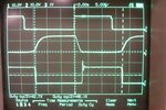
") I don't have Vds screen but I have the load voltage.
I don't have Vds screen but I have the load voltage.