Continue to Site

Welcome to EDAboard.com

Welcome to our site! EDAboard.com is an international Electronics Discussion Forum focused on EDA software, circuits, schematics, books, theory, papers, asic, pld, 8051, DSP, Network, RF, Analog Design, PCB, Service Manuals... and a whole lot more! To participate you need to register. Registration is free. Click here to register now.

[MOVED] Can someone explain this op-amp BPF circuit?

Status
Not open for further replies.

T3STY

Full Member level 4
Joined
Apr 17, 2012
Messages
239
Helped
24
Reputation
48
Reaction score
24
Trophy points
1,308
Activity points
3,715
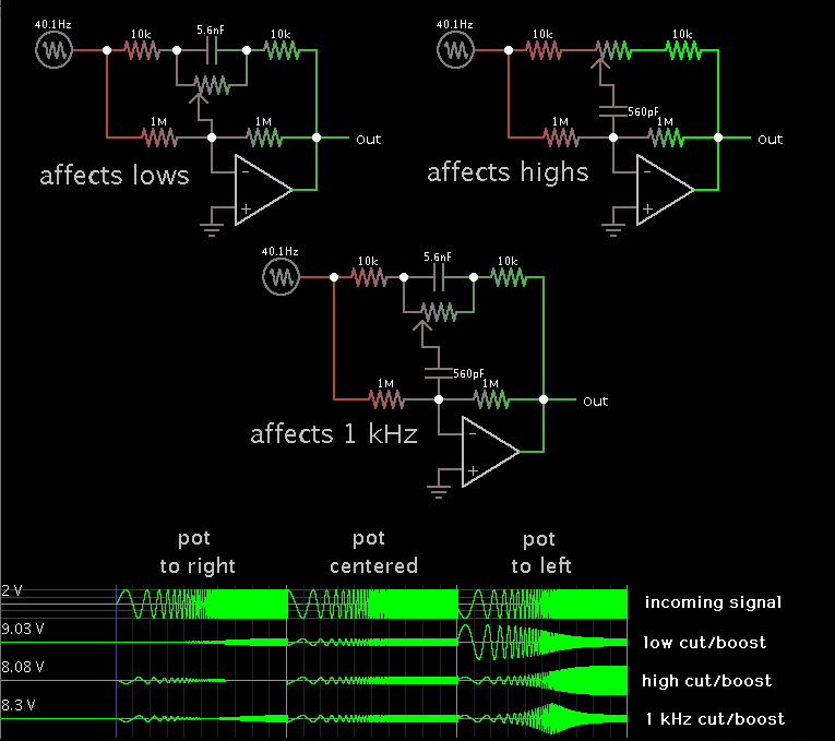
Some time ago I was looking for some ready-made band pass filter circuit that would be able to boost/cut the band. I found then a circuit which works just fine (simulated in ISIS), but I can't understand the logic behind of it because the author didn't explain it. Here's the link to the page where I found the circuit:

http://www.next.gr/audio/equalizers/octave-equalizer-circuit-l14813.html

A part from telling me anything I should know about it, my questions are:
1) Is this a multiple feedback design?
2) Where are the filters? I mean, I can't identify the components that actually make the filter while I still know that C1 and C2 are part of it.
3) If my suppositions are right, the feedback circuit is itself a filter. How does it impact on the whole?
4) Why does changing the value of R2 make the filter boost or cut, without affecting the band pass filter itself?
5) What do the 1MOhm resistors (R3) do? Placed there like this seem to have no particular purpose for the filter but changing their values to 10kOhm for example in ISIS would mess up everything; either the filter won't work at all or it would "work" but I would hear noises only.
6) How may I calculate the component values for a specific frequency? I know there are 10 bands already calculated, but it's for my personal interest.
7) What is (or how may I calculate) the bandwidth of this filter? The same for the Q factor.

I know I'm asking a lot.. actually, everything.. but please, I'm really interested in understanding this circuit.
Thanks to anyone who'll be answering!
 
Last edited:

4) Why does changing the value of R2 make the filter boost or cut, without affecting the band pass filter itself?

Yes, there is a lot going on here.

You can recognize how the potentiometer boosts or cuts gain.

Then the two capacitors act to create a band where the gain adjustment has its greatest effect.

The feedback loop has the lower capacitor in series. This use of a capacitor exaggerates the effect on highs. Lows are affected hardly at all.

As for the upper capacitor, the potentiometer not only varies gain, but it taps closer to either end of the upper capacitor. The ends show an opposite phase difference. (One end leads, the other end lags.) This use of the capacitor creates an exaggerated effect on lows.

So both capacitors introduce phase differences. One exaggerates highs, the other attenuates them. The net result on highs is that they are unaffected.
A similar concept applies to lows.

Therefore at frequencies where the phase differences null each other, that is the passband. It is the band of exaggerated effect.

5) What do the 1MOhm resistors (R3) do? Placed there like this seem to have no particular purpose for the filter

It appears you are correct. They are not needed although they may center the output at 0V if the input were to drift up or down.

6) How may I calculate the component values for a specific frequency? I know there are 10 bands already calculated, but it's for my personal interest.

The RC time constant applies here. Also the formula C = 1 / ( 2 x Pi x R x f ). At first it would look as though it should only involve the 100K pot, but there must be more to it than that because I get a different result. So perhaps the two 10K resistors must be included in the equation.
 
  • Like
Reactions: T3STY

    T3STY

    Points: 2
    Helpful Answer Positive Rating
To start understanding the circuit, imagine you build it but replace C1 with open circuit and C2 with short circuit. Now it is a simple inverting amplifier with variable feedback. By adjusting the potentiometer you can vary the voltage gain between about 0.1 to 10.

Now if you build it as shown, with the capacitors....

  • At very low frequencies C2 is effectively open circuit, so the potentiometer is disconnected from the feedback point and has no effect. The circuit becomes an inverting amplifier with unity gain.
  • At very high frequencies C1 is effectively short circuit. Since the potentiometer is short circuited, it has no effect and the circuit is again an inverting amplifier with unity gain.
  • However there is a band of frequencies in between where the impedance of C1 is high enough that the potentiometer is not completely shorted and the impedance of C2 is low enough to couple the potentiometer to the feedback point fairly effectively.

    In that band, adjusting the potentiometer will change the feedback factor and thus change the voltage gain of the circuit - in a similar way to when C1 was open circuit and C2 was short circuit, but not over such a wide range.

My math isn't good enough to calculate all the formulas but the capacitors are both proportional to 1/(center frequency). e.g. to double the frequency, you need to halve the value of both capacitors.
 
  • Like
Reactions: T3STY and FvM

    FvM

    Points: 2
    Helpful Answer Positive Rating

    T3STY

    Points: 2
    Helpful Answer Positive Rating
Supplementing godfreyl's intuitive analysis, it should be clear that other than said, R3 is of course affecting the filter characteristic as it forms a time constant with C2.

You'll recognize a basic similarity of the circuit with a MFB bandpass filter. But I fear, there's no inituitive way to determine the component values for an intended characteristic, except for the obvious way to scale the center frequency that has been shown by godfreyl. You'll need to refer to an exact calulation or use a circuit analysis program.

The present circuit dimensionining doesn't seem to be suitable for high end applications due to the rather high noise level, I also think that a multi-band equalizer should better use the well-known active inductor topology that has been often discussed at edaboard, the latest in a previous thread of the OP https://www.edaboard.com/threads/273488/
 
  • Like
Reactions: T3STY

    T3STY

    Points: 2
    Helpful Answer Positive Rating
T3STY,

in your first posting, several times you mentioned the term "bandpass filter".
May I point to the fact that the circuit shown is no bandpass at all.
The circuit has three different major transfer characteristics:
* Mid potentiometer position: Inverter operation with unity gain (no frequency dependence);
* Potentiometer at most right: "Weak" band-stop characteristic with only 12 db max attenuation and rising phase angle around the center frequency, 0 db gain for very low and high frequencies;
* Potentiometer at most left : "Weak" band-pass characteristic with only 12 db max gain and falling phase angle around the center frequency, again 0 db gain for very low and high frequencies;

The quality Q factor for this second order circuit is directly related to the maximum slope of the phase function (group delay magnitude at center frequency).

Here comes the formula: Q=0.5*wo*|d(phi)/dw| measured at w=wo
 
Last edited:
  • Like
Reactions: T3STY

    T3STY

    Points: 2
    Helpful Answer Positive Rating
Thank you all for the answers guys!

If I correctly understood Brad's analysis, the feedback circuit will do all filtering and as explained by FvM it has nothing to do with a multiple feedback design. While a part of the filter will affect the bands (boost/cut) the other will contrast this effect. Here I can integrate godfreyl's analysis, so when a specific range of frequencies is passing through the feedback circuit (near the central frequency), the gain will do its magic boosting or cutting the effect on them. Which then is further explained by LvW saying the feedback circuit will act as either band-stop or band-pass on the frequencies, resulting in a boost or cut.

Did i correctly understood you or am I missing the point?

@LvW: Well... I wasn't able to call it any differently and since I was searching on the web with the "bandpass filter" keyword I thought I could just consider it as this. Thanks for pointing that out though ;)
 

So that we all can see what concepts are at work here...

I made simulations of the equalizer circuit and two variations. The variations each have a capacitor removed to isolate the effects on frequency response.

Screenshot of the Falstad simulation:


I added text labels. The 1M resistors did turn out to be required after all.

The upper left circuit acts as a low frequency boost/cut. The active inductor (or gyrator) is at work somewhere here. No coil is needed.

The upper right circuit acts on the high frequencies only. Lows are not altered.

At the bottom is the equalizer circuit linked to in post #1. Capacitor values are for 1000 Hz.

It is easy to see the results, but not so easy to explain the interaction.
 
I got the same result too when I simulated it on ISIS. I hoped it would answer some of my questions but didn't, so I asked here.
Anyway, I think I had enough answers on this.. I mean, I understood what the circuit basically does. It would have been great if the original author explained it a bit and gave some hints on how to calculate components and how will they affect the whole, but as long as I'm not really interested on using this circuit or modifying it, I won't bother you anymore trying to understand someone else's logic then explain it to me.

Thank you again guys, I appreciate your efforts!
 

Status
Not open for further replies.

Similar threads

Part and Inventory Search

Welcome to EDABoard.com

Sponsor

Back
Top