ata90
Member level 5
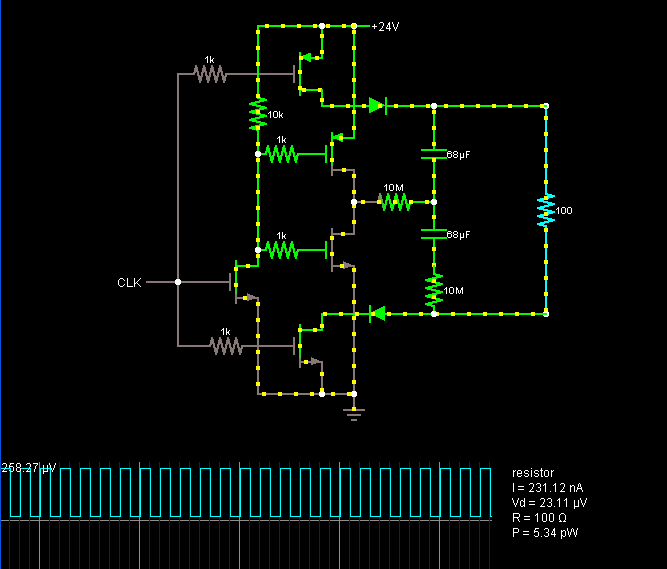
Dear all
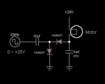
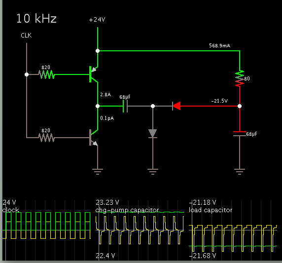
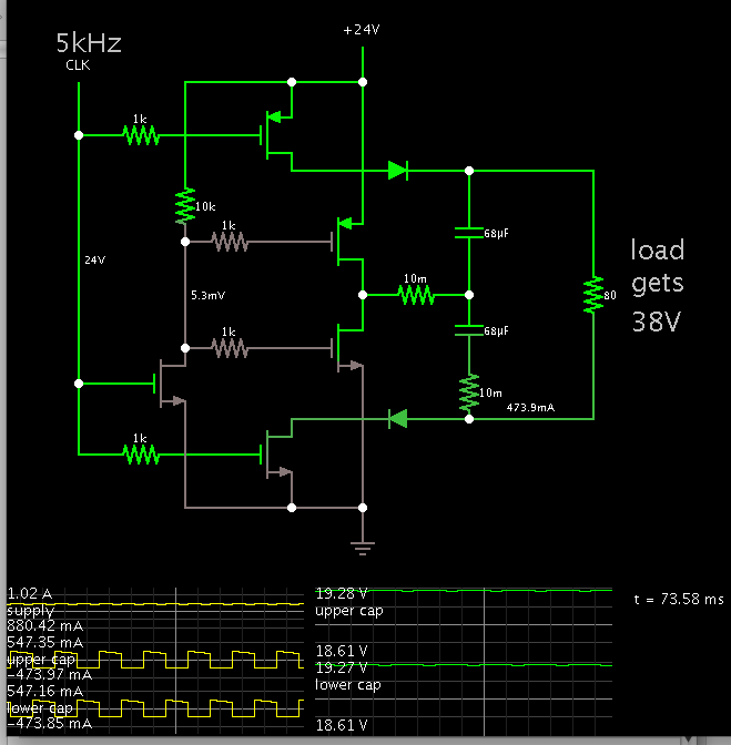
In order to run 48V, 0.6A motor with 24V power supply, I implemented circuit bellow which used charge pump and generated negative voltage. the voltage around the motor is near to 48V and motor works properly; but the problem is that both of 1N4007 diodes become too hot. is it the nature of these diodes to become hot at this current?

Thanks for any helps..
In order to run 48V, 0.6A motor with 24V power supply, I implemented circuit bellow which used charge pump and generated negative voltage. the voltage around the motor is near to 48V and motor works properly; but the problem is that both of 1N4007 diodes become too hot. is it the nature of these diodes to become hot at this current?
Thanks for any helps..