Continue to Site

Welcome to EDAboard.com

Welcome to our site! EDAboard.com is an international Electronics Discussion Forum focused on EDA software, circuits, schematics, books, theory, papers, asic, pld, 8051, DSP, Network, RF, Analog Design, PCB, Service Manuals... and a whole lot more! To participate you need to register. Registration is free. Click here to register now.

anti serial MOSFET -- source mating vs drain mating

Status
Not open for further replies.

richipedia

Newbie level 4
Joined
Oct 24, 2012
Messages
5
Helped
0
Reputation
0
Reaction score
0
Trophy points
1,281
Location
NRW, Germany
Activity points
1,326
Hello everybody,

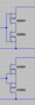
I am working on an application in which I need to employ a discrete MOSFET as a switch to block voltages of both polarities. I have already learned that because of the body diode, two MOSFETs connected in an anti serial manner must be used.
Now there are two possibilities: (see the picture below)
1. Connect both gates and both sources to form the switch. This is known as "source mating". (bottom of the picture)
2. Connect both gates and both drains to form the switch. This is known as "drain mating". (top of the picture)

Which option should be preferred, and why?
 

Attachments

  • sourcedrainmating.PNG
    sourcedrainmating.PNG
    3.9 KB · Views: 189

Do you mean block either a plus or minus voltage referenced to ground, or block a positive voltage referenced to ground in either direction?
 

I mean block both positive and negative drain-source-voltages.
Current flow is only in one direction.
 
Last edited:


crutschow: The gate is driven by a voltage between -1.8V and 3.3V. The signal comes from a cross-coupled level shifter I built myself.

Brad: Thanks for the link and the hint about the 4066. Unfortunately, the 4066 cannot withstand the max. 500mA current I need to sink.
 

crutschow: The gate is driven by a voltage between -1.8V and 3.3V. The signal comes from a cross-coupled level shifter I built myself.
The voltage to control a MOSFET is measured gate to source. For complete turn on, logic level types typically require 3.3V or 5V and normal types require 10V for Vgs.

What is the voltage level you are trying to block?

Post a schematic of the complete circuit you are proposing.
 

I used this setup with the sources coupled together, however this was a very high power application (several channels of 100+ Ampere's) and I used N-mosfets.
The reason I chose this setup was lower dissipation then with a P-mosfet since they have a higher RDSon.
I think it all depends on what power You want to switch, is it mA's or 100's of Ampere's.
 

Brad: Thanks for the link and the hint about the 4066. Unfortunately, the 4066 cannot withstand the max. 500mA current I need to sink.

This is the part I thought would be useful. You might be able to get discrete mosfets to work the same way. Don't know about the 3.3V however.


This is the part I thought would be useful. You might be able to get discrete mosfets to work the same way. Don't know about the 3.3V however.
Discrete MOSFETs will only work if you get those with a separate substrate connection and can can connect the substrates to their appropriate supply rails as the CMOS transmission gate does.
 

I fear, some contributions are missing the substance of the original question.
No ideas? Or does it not matter at all which type of mating I choose?
Of course it matters. I was neither aware of the "mating" terms nor do I see the purpose of "drain mating". If you refer to commecially available solid state relays, they are exclusively using connected sources (and mostly photovoltaic couplers to generate Vgs).

If it has any use, "drain mating" would be applicable for low switched voltage only, because it runs at risk to exceed Vgs otherwise.
 

Discrete MOSFETs will only work if you get those with a separate substrate connection and can can connect the substrates to their appropriate supply rails as the CMOS transmission gate does.

Then it sounds as though this has to be manufactured all on one piece of silicon, correct?

If so then the question comes up, is there a similar IC that can handle heavier current (as several have asked for in previous threads)?

Is a solid-state relay the answer?

The 4066 has been about the only ideal solution I've seen, for cases where we want to switch analog signals on/off. It's almost like a relay, only faster. I'm amazed it works like it does. The I/O pins conduct a signal in either direction. It's easily controlled by high/low voltage at the input pin. No need for tedious adjustments, etc.

I have not seen an arrangement of discrete components that will do the same so easily. I once tried to find a way to do it with diodes, transistors, etc. Could not succeed.
 

Then it sounds as though this has to be manufactured all on one piece of silicon, correct?

...........................
Not necessarily. You just need a P-MOSFET and N-MOSFET with a separate connection to the substrate of each device. Here is an example of such a P-MOSFET device.
 
To remember the anti-serial topology, as asked in the original post:


Of course, the photovoltaic coupler could be replaced by a direct connected (floating) gate voltage source.

The discussed parallel CMOS switch works different. It depends on separated source and substrate nodes and can't be implemented with usual power MOSFET devices.
 
crutschow: This is basically what I want to do:

The "source" of my switch S0 is tied to ground. The "drain" voltage is 4.2V when S2 is closed, -1.8V when S1 is closed, or ~0V when S0 is closed. Current flow direction is indicated by the current source (max. 500 mA).
As gate voltages, I have 3.3V and -1.8V available. 3.3V is more than enough to turn the NXP NMOS in this circuit on: **broken link removed**
The targeted switching frequency for my circuit is somewhere between 1 and 5 MHz. I know that's a though specification, but it's possible.
Thank you for the PMOS with seperate bulk connection, but it seems like a NMOS with bulk connection is even more difficult to find.
 

Your circuit can short a voltage input to ground if one of the switches and the MOSFETs are on at the same time, which is a no-no. Can that occur?

Also the gate input voltage must be equal to the highest source voltage to insure complete turn-off of the MOSFETS. Thus the V_control high voltage must be ≧V2.

To answer your original question, offhand I don't see any difference in which order the MOSFETs are connected.
 

Status
Not open for further replies.

Similar threads

Part and Inventory Search

Welcome to EDABoard.com

Sponsor

Back
Top