Continue to Site

Welcome to EDAboard.com

Welcome to our site! EDAboard.com is an international Electronics Discussion Forum focused on EDA software, circuits, schematics, books, theory, papers, asic, pld, 8051, DSP, Network, RF, Analog Design, PCB, Service Manuals... and a whole lot more! To participate you need to register. Registration is free. Click here to register now.

question: LDO pass device and input offset voltage

Status
Not open for further replies.

cmos_ajay

Full Member level 2
Joined
Jan 30, 2007
Messages
126
Helped
0
Reputation
0
Reaction score
0
Trophy points
1,296
Activity points
2,247
question: LDO pass device and input offset voltage ?

Hello,
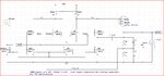
Attached is a picture of an LDO schematic seen in the IEEE paper: A 1.21V, 100mA, 0.1uF - 10uF output capacitor LDO voltage regulator for SOC applications. The vref is a bandgap voltage (1.2V) and the resistors R1 and R2 are adjusted to deliver the desired output voltage (2.5V). The VDD = 3V

The output PMOS pass device (Mpass) is made large enough to handle a desired load current.
* Under DC conditions, when there is no load connected (I_load = 0), an input offset voltage is observed.
** Is there any solution to prevent the input offset voltage ??
 

Attachments

  • ldo_schematic.JPG
    ldo_schematic.JPG
    131.6 KB · Views: 108
Last edited:

That amplifier will have too low a gain to give good offset,
or load regulation. It has to bury the mirror just to get you
to a good low current. You also limit the drive to the pass
FET to (VDD-vref-VTN) and at this point the amp gain is
pretty poor; you'll suffer in load regulation at the big end,
from that.

I'd say you want another stage worth of gain and it
should be rail-rail swing at the pass FET gate. Otherwise
you use less of the "dynamic range" of the FET and have
to tolerate either more leakage, or less max current,
than you could get.
 

Hello dick_freebird,

"It has to bury the mirror just to get you to a good low current."
* Can you please explain this better and Which devices in the mirror are you referring to ?

"You also limit the drive to the pass FET to (VDD-vref-VTN)"
* As seen in the figure, the overdrive voltage of Mpass is [(VDD - VR) - Vtp ]. Can you tell why it is (VDD-vref-VTN) instead ??

Thanks.
 

M4 has to turn the pass device off, it is the only one
that can. And to do that, its Vds <= Vgs; puts it linear
and drops stage gain big time.

M2 turns it on, M2 drain can go no lower than Vreg-Vtn,
M2 drain can go no lower than source (Vref-Vtn) and
the pass FET Vgs = (Vref-Vtn)-Vdd (magnitude =
Vdd-Vref-Vtn) ). In regulation, that is.
 

Do you have another schematic since you said "I'd say you want another stage worth of gain and it
should be rail-rail swing at the pass FET gate."
 

I don't have one handy, but I'd suggest a folded cascode
with rail-rail output stage, and biased such that you get
as much saturated range as possible (at DC - you may
want to look at boosting the bias at high error positions,
for step / slew response).
 

Status
Not open for further replies.

Part and Inventory Search

Welcome to EDABoard.com

Sponsor

Back
Top