Continue to Site

Welcome to EDAboard.com

Welcome to our site! EDAboard.com is an international Electronics Discussion Forum focused on EDA software, circuits, schematics, books, theory, papers, asic, pld, 8051, DSP, Network, RF, Analog Design, PCB, Service Manuals... and a whole lot more! To participate you need to register. Registration is free. Click here to register now.

how to bias the integrator

Status
Not open for further replies.

prcken

Advanced Member level 1
Joined
Nov 1, 2006
Messages
419
Helped
41
Reputation
82
Reaction score
37
Trophy points
1,308
Location
Shanghai
Activity points
4,059
in Razavi's CMOS book Chapter 12, see figure below
Capture.PNG
how to bias the opamp properly since the opamp is configured with capacitive feedback (C2) at both phases?
thanks!
 

Diagram B shows the first part of the cycle from diagram A. The switches are in one position.

Diagram C shows the second part of the cycle. The switches are in the other position.

The switching speed is several times faster than the incoming signal. Somehow it acts as a filter, but I have not learned exactly how.

The schematic is similar to one in the animated interactive simulator at falstad.com.

Click the link below. It will open the website, load the schematic and run it on your computer. (Click Allow to load the Java applet.)

https://tinyurl.com/anq63y8

You can alter the circuit by right-clicking on a component. This will bring up an edit window.

You can delete the plain feedback wire and change it to a capacitor. (I believe it changes the output amplitude at a certain range of frequencies).

This circuit is listed under 'Active Filters' only in the downloadable version of the simulator. It does not appear in the list of circuits found at the website.
 

It is a switched-capacitor circuit. The switched capacitors, which are switched at a much higher speed than the signal frequency, simulate resistors, i.e. the charge carried through the switched capacitor is proportional to the voltage across the switched-capacitor circuit. The equivalent resistance of the switched capacitor circuit is inversely proportional to the switching speed times the capacitor size. Thus, the integrator is biased the same as if the switched-capacitor input was actually a resistor.

Switched capacitors are used in ICs because it's easier and takes less space to build precision capacitors then it is precision resistors in the standard IC process.
 
in Razavi's CMOS book Chapter 12, see figure below
View attachment 82262
how to bias the opamp properly since the opamp is configured with capacitive feedback (C2) at both phases?
thanks!

Normally, such a circuit (classical S/C integrator topology) is used not as a stand-alone circuit but it is a part of an overall negative feedback loop (filter circuit).
In these cases, no special bias considerations are required. This is the same situation as for continuous time integrators, which also cannot be operated without an overall negative feedback loop.

Yes, that's what i am confused about, there is no DC feedback loop for the opamp.

- - - Updated - - -

hi BradtheRad, the animation is interesting, thank you

- - - Updated - - -

It is a switched-capacitor circuit. The switched capacitors, which are switched at a much higher speed than the signal frequency, simulate resistors, i.e. the charge carried through the switched capacitor is proportional to the voltage across the switched-capacitor circuit. The equivalent resistance of the switched capacitor circuit is inversely proportional to the switching speed times the capacitor size. Thus, the integrator is biased the same as if the switched-capacitor input was actually a resistor.

Switched capacitors are used in ICs because it's easier and takes less space to build precision capacitors then it is precision resistors in the standard IC process.

Hi crustchow, thanks for your reply. yes, it's SC circuit, i know its application and its block diagram function. just one doubt about how to DC bias the opamp with feedback, or just as LvM said there is no need to use feedback to bias the opamp here in this case, maybe use another pair of switches with an input bias voltage at appropriate phase for input common mode and the output common mode is set internally by CMFB? what i meant is for fully differential application.
 

Hi crustchow, thanks for your reply. yes, it's SC circuit, i know its application and its block diagram function. just one doubt about how to DC bias the opamp with feedback, or just as LvM said there is no need to use feedback to bias the opamp here in this case,....

Just in order to avoid a misunderstanding: There is no need for separate bias considerations if the S/C integrator is used as one element in a closed negative feedback loop which contains also other stages (like in active S/C filters).
 

Just in order to avoid a misunderstanding: There is no need for separate bias considerations if the S/C integrator is used as one element in a closed negative feedback loop which contains also other stages (like in active S/C filters).

Hi LvW, I do not quite know how S/C integrator is used in active filters, i guess it has several integrator stages in cascade, and it forms a closed negative feedback from the last stage to the first stage. so that the latter stage can bias the former stage well.
here i am trying to do opamp sharing in a pipeline ADC, it is cascade stages, but there is no feedback like the case i said before.
 

here i am trying to do opamp sharing in a pipeline ADC, it is cascade stages, but there is no feedback like the case i said before.

In this case, I think, you should follow the same guidelines as in the analog domain: Use a damped (lossy) integrator (Resistor Rp in parallel to the feedback C) which resembles a 1st order low pass filter.
In the sampled-data domain (S/C technique) the resistor Rp is, of course, realized as another switched capacitor.
Could this cure your problem?
i have to think more, since the opamp is working(at amplification mode for stage one and stage two) at both phases, there is no time for another SC as a resistor, i think....
 

..............................
here i am trying to do opamp sharing in a pipeline ADC, it is cascade stages, but there is no feedback like the case i said before.
What is the purpose of the integrator in the pipeline ADC? Don't you just need the op amp as an amplifier?
 

What is the purpose of the integrator in the pipeline ADC? Don't you just need the op amp as an amplifier?
it's not used as the purpose of integrator but it will have the same configuration like the integrator figure (there is a cap at both phases there ) mentioned above during both phases for stage 1 and stage 2 in the pipeline if the opamp is shared.
 

it's not used as the purpose of integrator but it will have the same configuration like the integrator figure

I think, when a circuit has the configuration of an integrator (with or without intention) it will work as an integrator, will it not?
 

I think, when a circuit has the configuration of an integrator (with or without intention) it will work as an integrator, will it not?

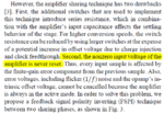
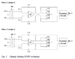
Yes, i said something wrong, you are right. I should say my case is a precision multiply-by-two circuit in the 10-bit pipeline ADC stages, when two stages share an opamp, there is always a cap feedback around the opamp, so that there is no time for DC feedback to bias the opamp properly.

- - - Updated - - -

i think i have found a paper discussed about this issue "A 69-mW 10-bit 80-MSample/s Pipelined CMOS ADC" IEEE JOURNAL OF SOLID-STATE CIRCUITS, VOL. 38, NO. 12, DECEMBER 2003.
Capture.PNG
Capture2.PNG
Capture3.PNG
but what it said is nonzero voltage instead of how to bias the opamp which i am not quite understand.
 

Looking at the schematic, it seems obvious that it's simplifying things a bit. No MOSFET or BJT amplifier can work without a switched or continuous input bias path. I don't think that it makes sense to discuss circuit details at this level of superficial knowledge.
 

Looking at the schematic, it seems obvious that it's simplifying things a bit. No MOSFET or BJT amplifier can work without a switched or continuous input bias path. I don't think that it makes sense to discuss circuit details at this level of superficial knowledge.

yes, those switches are simplified at each phase.
 

Status
Not open for further replies.

Similar threads

Part and Inventory Search

Welcome to EDABoard.com

Sponsor

Back
Top