themaccabee
Full Member level 4
Hi,
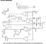
Im working with a buck converter design..The part is LT3508..running at 700kHz ...it has two regulators in a single package with integrated switch for each.
It has a boost pin which is connected to the output voltage node and this is done to drive the internal NPN switch to saturation and there by helping in efficiency..Im using one regulator for generating 3.3V/400mA output.
My question is how to find the dissipation in diode D2. I think for diodes it is usually specified like I x Vf ...( assuming Vf change w.r.t I is negligible)..Now the problem comes like how to approximately find the average diode current..through D2?
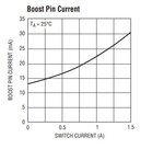
I believe the lower node of C3 willl experience 24V and 0V at the switching cycles..and the lower node of D2 is 3.3V regulated..and in normal working conditions the capacitor C3 will be charged to 3.3V approximately...The BOOST pin current is very low usually.. around 20mA at 25degree @0.5A output current..
Can any body help me??


Last edited: