Continue to Site

Welcome to EDAboard.com

Welcome to our site! EDAboard.com is an international Electronics Discussion Forum focused on EDA software, circuits, schematics, books, theory, papers, asic, pld, 8051, DSP, Network, RF, Analog Design, PCB, Service Manuals... and a whole lot more! To participate you need to register. Registration is free. Click here to register now.

[SOLVED] Altium art work problem

Status
Not open for further replies.

midohamaki

Newbie level 5
Joined
Nov 13, 2010
Messages
8
Helped
0
Reputation
0
Reaction score
0
Trophy points
1,281
Activity points
1,340
hi guys ..
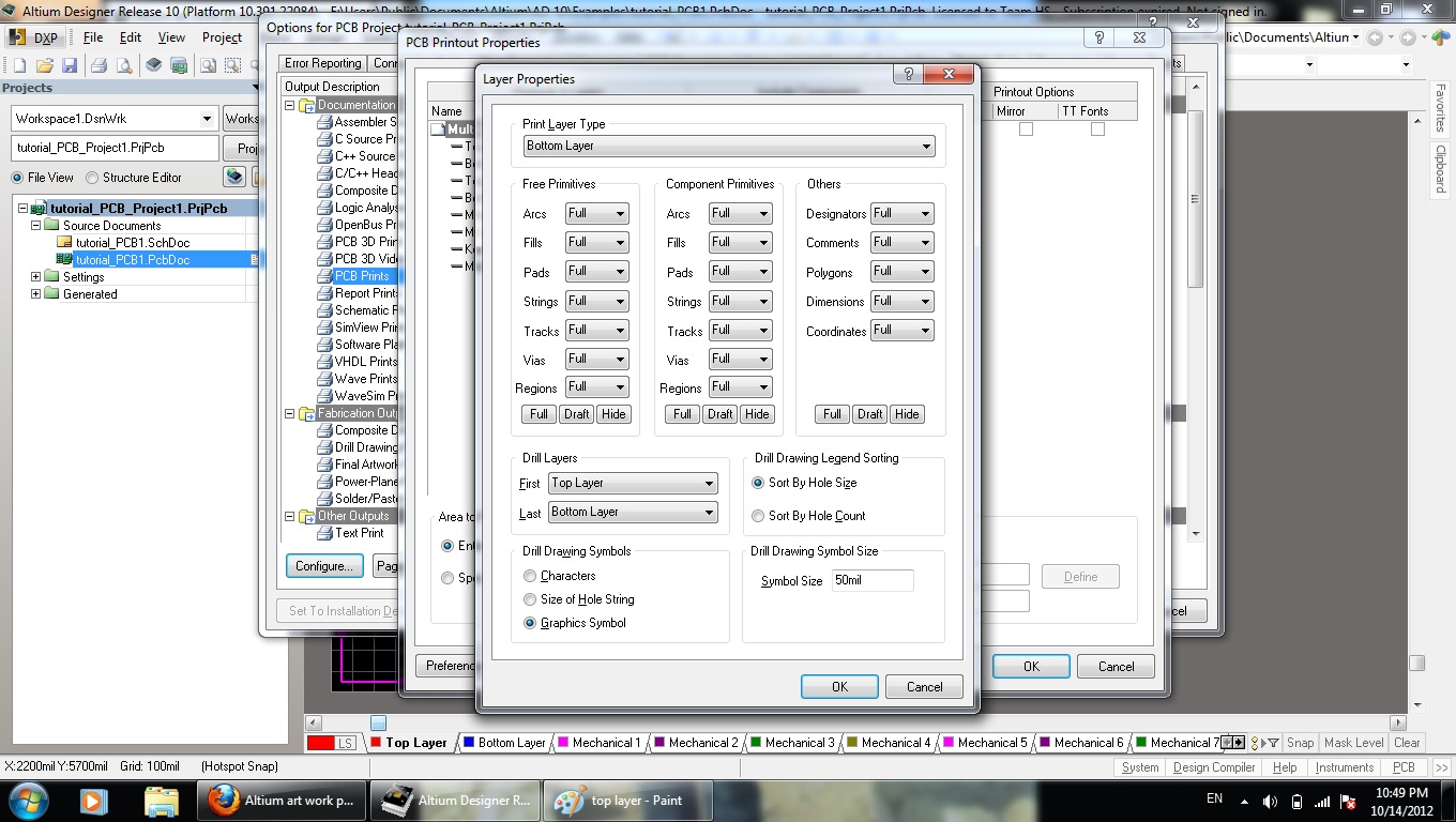
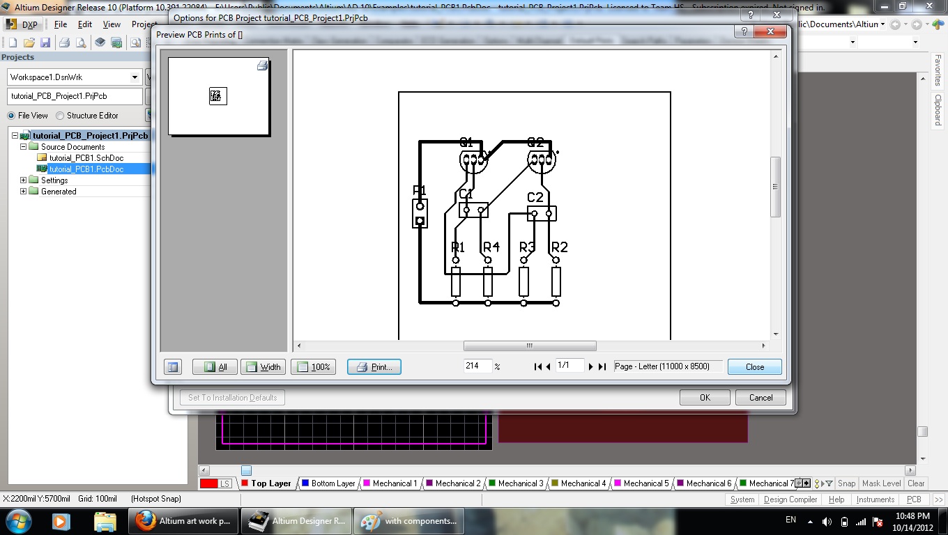
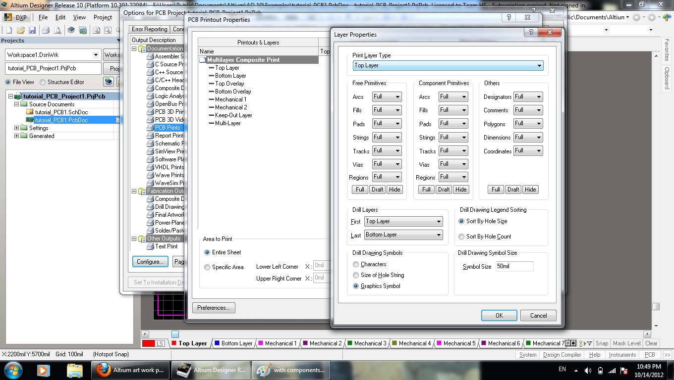
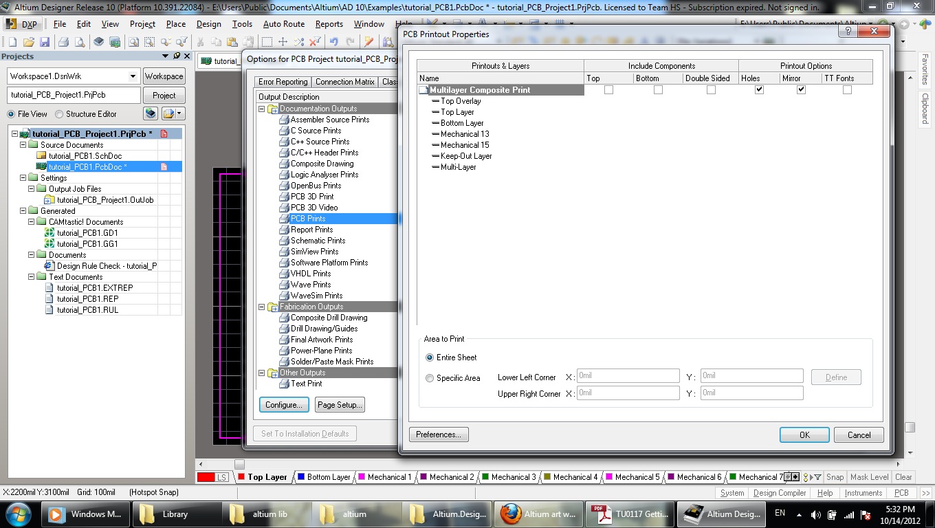
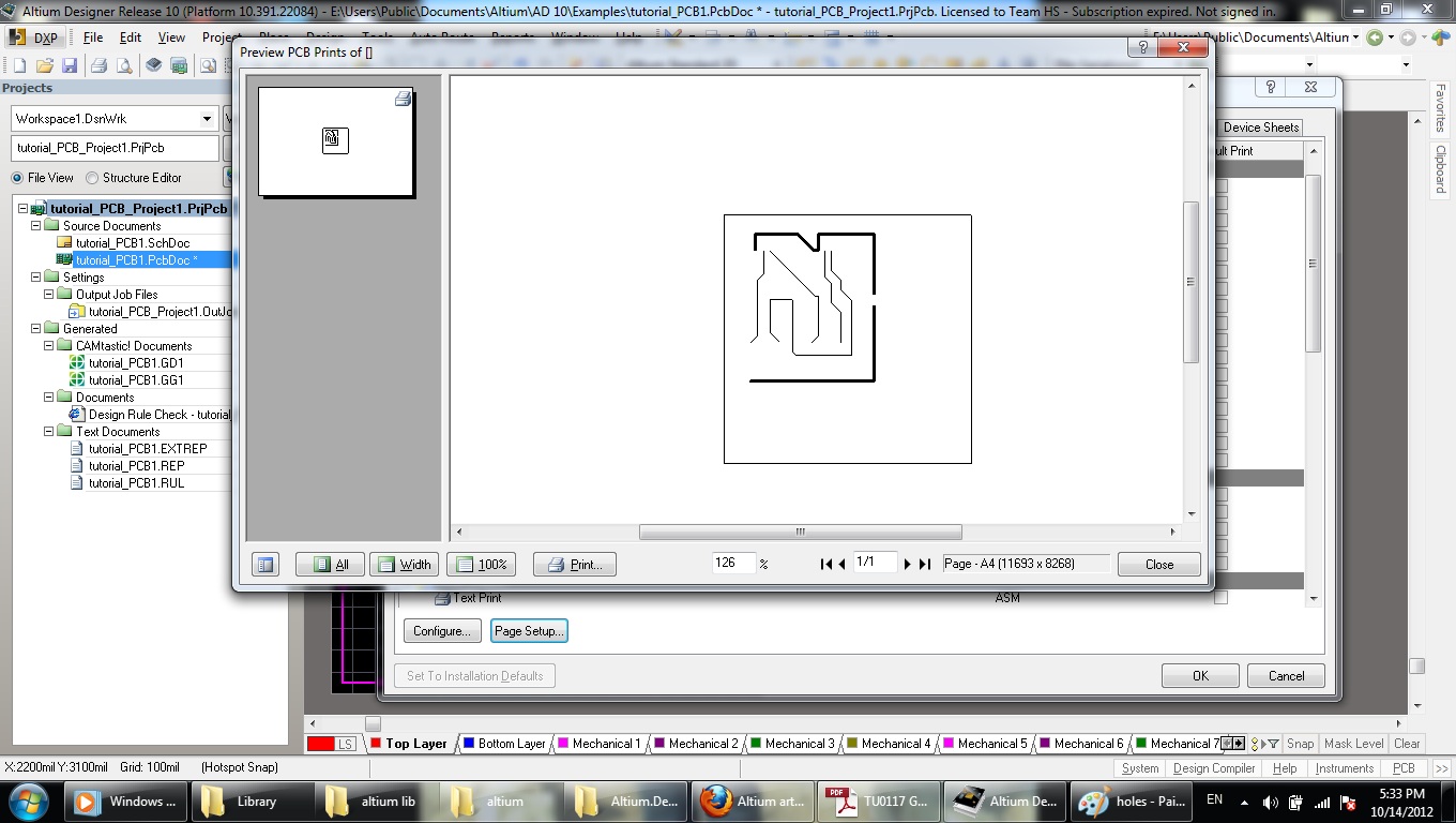
i am using toner transfer method for PCB and Altium design software ,
but i can not get printed circuit scaled to components from Gerber file
i do not know what to do >>> any help plz
thnxxxx
 

You don't print from gerber file becuase you don't get the holes, Goto project from the top bar then goto project options this open's diaglog box goto default tab prints then look for PCB prints then click on the configure button at the bottom turn off the layers you don't need to print click on holes then page setup then look for scale mode rather than fit document and then mono then print
Sorry for quick reply if you still can't do it then I will write it a bit more indepth but off out now
 
Thnxxx WIZPIC
the problem now is in scaling what is the scale of the page make it fit with the component's i tried a lot but nothing work
and when i choose holes option it not apear in print preview and if i clicked on top at components included
it's appear but with component's which i do not want to appear
thnx for your efforts and your time
 
Last edited:

Have a look at the pic you slelect scale 1:00 as long your board will fit on A4 if it all does not fit on A4 like you get the board spread over 2 sheet try changing the it landscape or portriat which depends on how you've got it set now
Config1.JPG

This is the way I do it let me know how you go with it

wizpic
 

i know the circuit gonna fit with the paper but is it gonna match the real dimension of he component's in 1:00 scale ??
and i clicked on holes and do not appear too


Make sure your set up is like this, Just double click on each of the multilayer EG top layer turn off all and then do the same on the bottom layer (like picture) make sure everything is turned onto full like(config2 pic)
The same has for the multi-layer(config3) and it should come like like the pic in config4
By the looks of it you have not enabled all like in pic config6 becuase it turns out like pic config5
config2.JPG
config3.JPG
config4.JPG
config6.JPG
config5.JPG
 

i did every thing u told me and there is no thing change :( i do not no from where came my wrong !!!!
and i print the circuit in 1 scale and it did not match the dimensions of the components !! ??
why is that too sry for buzzing you but i need serious help
thnx
 

Youre nearly there It looks one to one to me looking at your pic you are 214% zoomed in the only thing you need to do is trun of the top overlay like in my pic

top overlay.JPG

My advise would be to alter the pad size and hole has there is not a lot of meat on them and your pcb may not etch, Altium have some good video's on there site, kep going your nearly there Alitum has got a very steap learning curve but so easy to use once you have mastered it
 
Thank you so much :) i will try and error the scale until i can fit it and post the result
and last thins is the transistor out line is appearing after i turned off top overlay layer how can i fix that
you are great man
 

Have a look at mechanical layer'a 1&2 and do the same turn them all off do the same for the bottom overlay

It look to scale to me if you are talking about that it is closse to the edge look at the pic in post 4 and see where it said margins untick center and and use the little buttons to move it to center, lookig at one of the pics you posted it was centered and looking at the last one you posted you have changed it from A4 to letter this could also be one of the reason it's not prining in the center now
 

WIZPIC :) you are the man
I DO not know how to thanks you Really the Problem solved with turning mechanical layers off and a bout the scaling tomorrow i will match it with the IC's and any other components to figure out the correct scaling .
i hope to accept me as your a students
thaaaaaaaaanks

- - - Updated - - -

i measured and make a lot of try and error and find that the best scale is 1.00 and you was right from start but i was not sure of it
thaaaanks wizpic :)
 

your welcome we are here to help, Been using altium for years and i still am learning new things and short cuts

need any more help and i will see if i can help
wizpic
 
Status
Not open for further replies.

Part and Inventory Search

Welcome to EDABoard.com

Sponsor

Back
Top