sabu31
Advanced Member level 1
Hi
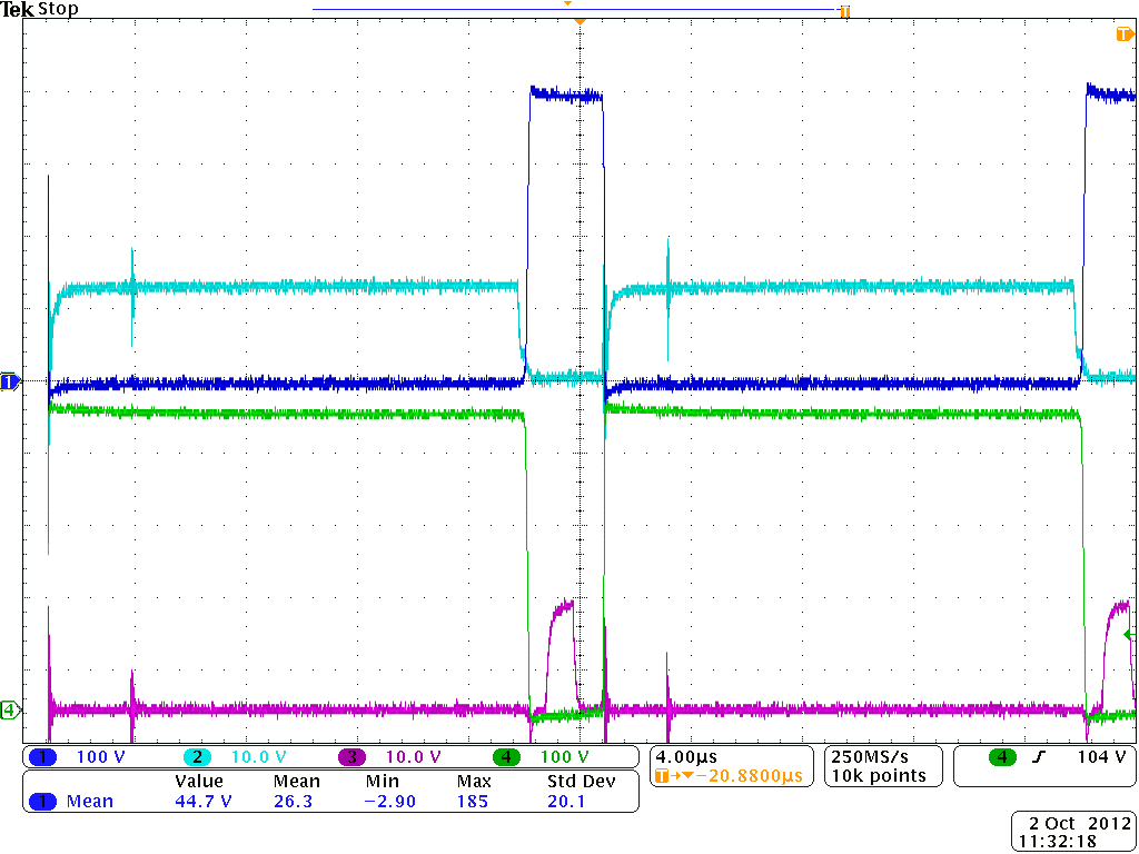
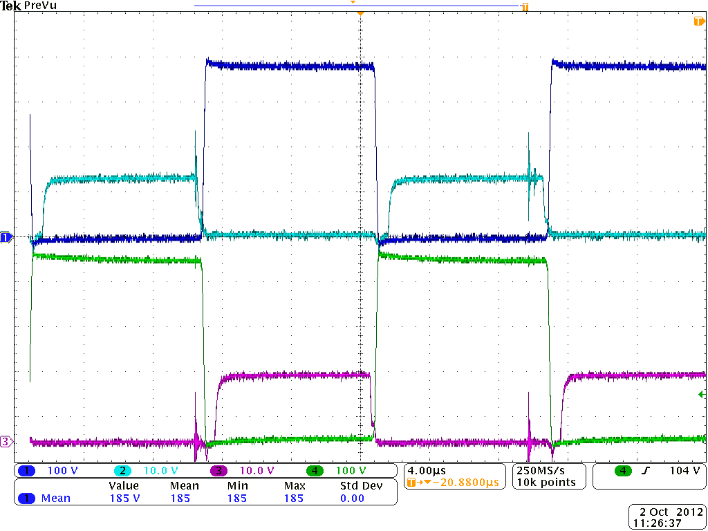
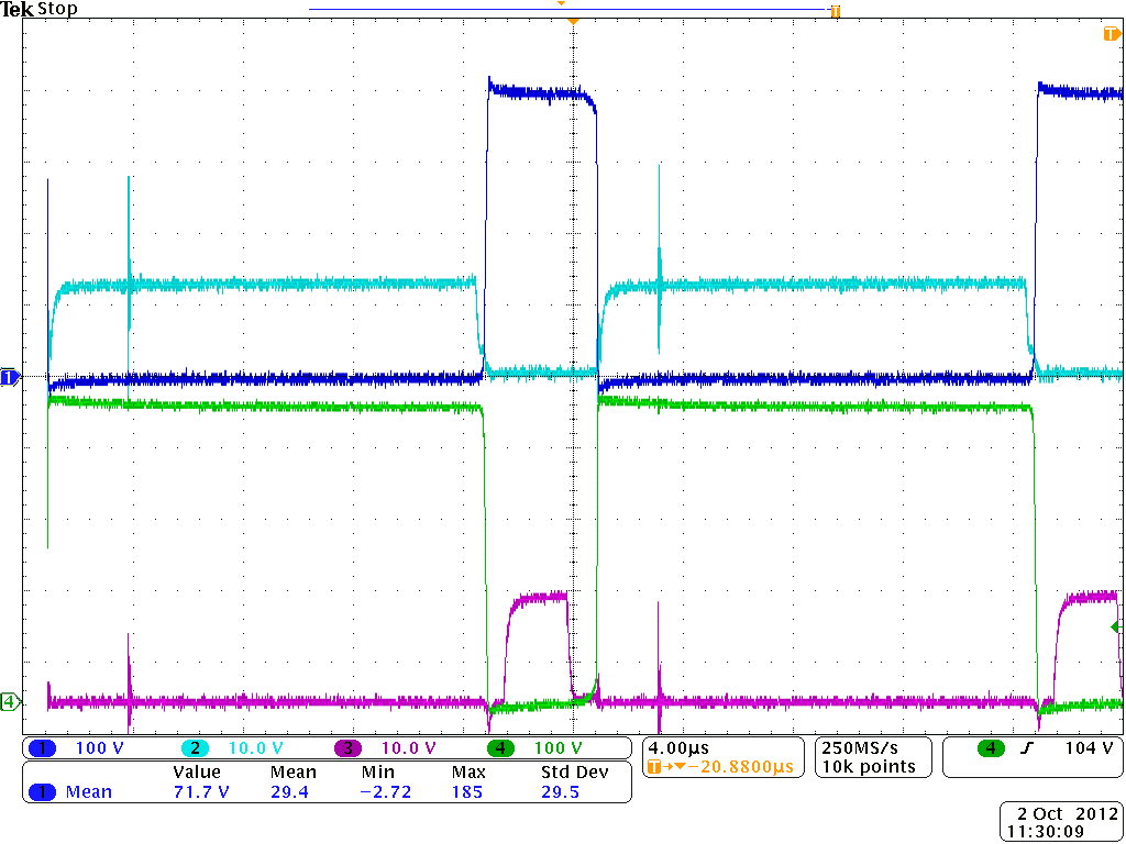
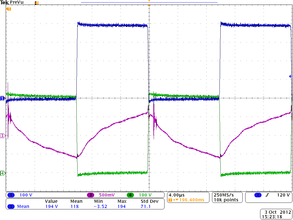
I am designing a 250w sine pwm inverter(H-Bridge). The dc link voltage will be 400V volts. And output required is 230Vrms.
I am driving the inverter using IR2110 and the switches used are IRFPE50PBF. The pwm frequency is 50kHz. However on runnning the devices gets heated within a minute. I tried simple square pwm with 50% duty ratio ,50Khz. This time no heating was observed. I wanted to know what could be the cause of heating, whether its due to conduction loss (Rdson=1.2 ohm) or whether its due to anti parallel diode(trr=980ns). I put a dead band of 1micro second.How do i reduce the heating.Is reducing the switching frquency the only method to reduce the heating .
, are there better devcies rated for 50kHz, and 1kW operation.
thanking you.