Continue to Site

Welcome to EDAboard.com

Welcome to our site! EDAboard.com is an international Electronics Discussion Forum focused on EDA software, circuits, schematics, books, theory, papers, asic, pld, 8051, DSP, Network, RF, Analog Design, PCB, Service Manuals... and a whole lot more! To participate you need to register. Registration is free. Click here to register now.

the modelling problem

Status
Not open for further replies.

power_pwer

Junior Member level 1
Joined
Jun 11, 2012
Messages
17
Helped
0
Reputation
0
Reaction score
0
Trophy points
1,281
Activity points
1,415
hello,everyone
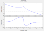
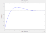
i am facing a problem that make me confused when i am modeling a voltage-mode buck converter.i got a phrase margin of 67degree as the figure"bode_67"shows,however i got a step response as the figure"step_67" shows.
the two plots comfuse me a lot because many meterial told me that the output response would rise up slowly to the final value as long as the phrase margin is higher than 60degree.but figure "step_67" shows a overshoot when its phrase margin is 67.
why does my plot conflict with that conclusion? can anyone help me?
 

Attachments

  • bode_67.png
    bode_67.png
    11.2 KB · Views: 60
  • step_67.png
    step_67.png
    8.2 KB · Views: 51

At first I was going to say it is due to resonant action between the coil and capacitor. This can happen if the On-time is long enough.

However when I look at your image named step_67... It appears to graph the first few cycles after power-up (the first 8 * 10 ^ -5 sec).

I am guessing that the peak is in the first few cycles? Because I find that when power is first applied to the buck converter, the output often soars in the first few cycles. It's due to the initial current surge on power-up. It is more pronounced when the capacitor is a high value.

This may or may not be relevant to the core issue of your question.
 

How do you derive the transfer function? Does the calculation consider modulator dead-time? Is it a synchronous buck converter, so you can be sure about a constant gain versus duty cycle?

It would be helpful to see a schematic with essential circuit parameters.
 

thank you,bradtherad and fvm,thanks for your replying
there is no schematic,i just model the converter with simulink,and i do both the bode plot and step response with simulink.the converter is synchronous with constant frequency clock turning on the power switch. the figures of the converter are: VI=12V;VO=5V;fs=100kHz;L=16uH;C=540uF;RO=0.5ohm;Vp=2V(Vp is the peak value of the sawtooth)
the following are my steps to derive the transfer function:
1,divide the converter into three part:LC filter,modulator and compensator
2,the transfer function of LC filter is (1/LC)/(s^2+s/RC+1/LC)
3,the transfer function of the modulator is VI/Vp;
4,use type3 compensator for the compensation(as figure"compen" shows)
5,i set a zero in the type3 compensator at the the crossover frequency of the converter to get a phrase margin higher than 45.
figure "loop gain" and "feedback loop" show how the bode plot is from and how the step response is from respectively.
 

Attachments

  • compen.png
    compen.png
    6.9 KB · Views: 51
  • loop gain.png
    loop gain.png
    4.6 KB · Views: 61
  • feedback loop.png
    feedback loop.png
    5.5 KB · Views: 53

Sorry I'm not more familiar with this field so I could be of more help.

Here's an article discussing voltage mode control in buck converters, type III compensation, and phase margin.

It shows graphs that resemble yours, with references to poles, zero's, loop gain and loop phase.

This quote might be relevant:

"A target of 50° to 60° for this parameter is considered ideal. Indeed, for a second order system with single-loop control, phase margin is directly related to transient response and a phase margin of 52° results in closed loop-peaking factor Qo of unity..."

https://www.edn.com/design/analog/4...-compensation-Intricacies-for-buck-regulators
 

    V

    Points: 2
    Helpful Answer Positive Rating
I forgot to ask a simple question: Is the shown step response belonging to the same linear model that's shown in the bode plot?

I presume it is. If so, the example just shows the limit validity of the simplified phase margin criterion. The steep phase characteristic around the filter resonance frequency also shows in the step response. You'll notice that a frequency estimation of the overshoot will end up around 10 kHz, just the filter peak in bode plot.

The other point mentioned in my first post should be considered though. VI/Vp isn't the complete modulator transfer function, usually an (average) dead time of a half switching period is assumed for a voltage mode controller. It causes a negative phase margin when applied to your design. In other words, besides the discussed overshoot problem, the controller won't work in a real design.
 

    V

    Points: 2
    Helpful Answer Positive Rating
thank you for both of your replying.
FvM,what do you mean by "the limit validity of the simplified phase margin criterion"?it is the first time i heard this.could you recommend me some merterial talking about this?
and thank you for your advice about my modulator gain transfer function.what is the "dead time of a half switching period"?
 

The derivation of the criterion "57 degree phase margin = no overshoot" refers to a first order loop with an additional pole and respective monotone phase response. I guess you can imagine that a resonator in the loop gain located near to the loop bandwidth shows in the closed loop response.

An exact analysis of a switched mode circuit requires to consider it's time discrete nature, because the error signal is sampled by the modulator. You are already using a time-continuous equivalent circuit when calculating with a modulator gain. But the deadtime caused by the sampling delay also affects the loop response. Calculating with a half switching period (5 us in your example) has shown suitable for voltage mode controllers that are basically averaging the error signal. As a result, you'll get 25 degree phase margin instead of 67 degree at the crossover frequency of about 23 kHz shown in your simulation.

I would perform a transient simulation of a time discrete switching regulator model to check the estimation.
 
thank you,FvM,you advices are very helpful
 

Status
Not open for further replies.

Similar threads

Part and Inventory Search

Welcome to EDABoard.com

Sponsor

Back
Top