nelly1
Junior Member level 3
hello everyone,
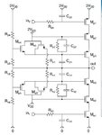
about this circuit attached i have several questions:
1.for the upper pmos stacked part: when the input is 2VDD, i think Mn4 should be off and Mn5 should be on.but what is the Gate voltage for Mp3?
2.for the nmos stacked part ne book said, "static efficiency of 90% ,which means that the output is not completely charged or discharged to 3 VDD or gnd respectively. The ratio of Rnp1 on Rnp2 and Rnp3 on Rnp4 equals 0.850 and 0.425 respectively."
dont get it.... how come 1 and 0.5 to 0.85 and 0.425?????
3.the capacitors Cnp1 are connectedin parallel with the gate-drain capacitances of the transistors Mnp3,which are not constant during operation.
even i know C1(total)*R1=C2*R2. how can we determin Cnp1???
Thanks in advance!

about this circuit attached i have several questions:
1.for the upper pmos stacked part: when the input is 2VDD, i think Mn4 should be off and Mn5 should be on.but what is the Gate voltage for Mp3?
2.for the nmos stacked part
dont get it.... how come 1 and 0.5 to 0.85 and 0.425?????
3.the capacitors Cnp1 are connectedin parallel with the gate-drain capacitances of the transistors Mnp3,which are not constant during operation.
even i know C1(total)*R1=C2*R2. how can we determin Cnp1???
Thanks in advance!
