Continue to Site

Welcome to EDAboard.com

Welcome to our site! EDAboard.com is an international Electronics Discussion Forum focused on EDA software, circuits, schematics, books, theory, papers, asic, pld, 8051, DSP, Network, RF, Analog Design, PCB, Service Manuals... and a whole lot more! To participate you need to register. Registration is free. Click here to register now.

[SOLVED] Buck-boost converter (DC/DC)

Status
Not open for further replies.

ohm77

Newbie level 4
Joined
Aug 9, 2012
Messages
6
Helped
0
Reputation
0
Reaction score
0
Trophy points
1,281
Location
montreal,canada
Activity points
1,327
Hi all,
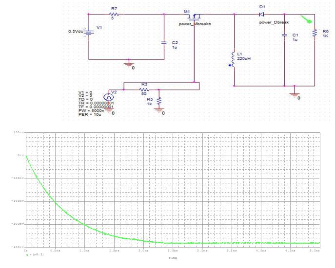
I'm working on a buck-boost converter (DC/DC), the specifications are: for 0.5V in the input I must have 3v in the output, and for the amplitude of oscillations that excite the grid of the transistor NMOS it must be less than 3v (the output voltage).
My problem is that when I give to the amplitude of oscillations 2.5v (that exite the grid of NMOS) it affects the output of the converter thus I get 1V at the output of my converter.
My question is: How can I get 3V in the output of the converter, and have an amplitude of oscillation less than 3v to excite the grid of the NMOS?
thank you. Capture01.jpg
 

Tips:

Reverse the direction of the diode.

Reduce (or remove) R1 and R7.

Increase (or remove) R2.

It will be surprising if you can get any output when your supply is 1/2 V.
 
  • Like
Reactions: ohm77

    ohm77

    Points: 2
    Helpful Answer Positive Rating
Your schematic shows an inverting buck-boost converter topology, with wrong switch transistor polarity (N rather than P) and reversed diode, as said. A regular boost converter should serve your purpose https://en.wikipedia.org/wiki/Boost_converter

You are mentioning a NMOS transistor but placed a N-JFET in your schematic.
 
  • Like
Reactions: ohm77

    ohm77

    Points: 2
    Helpful Answer Positive Rating
Hi, thank you so much, you gave me new ideas

- - - Updated - - -

I considered all informations that you gave me, I reversed the diode, and I tooked a NMOS transistor (power_Mbreak on pspice), I changed the value of some resistances as BradtheRad told me.
In the set of specifications, I must work with a buck-boost converter, I know that a boost converter can serve my purpose, but I have to respect the requirements.
when I made changes in the 1st schematics, I got the output below.
In the set specifications I must have 3V (until 3.3V) in the output, but it's not what is shown below.
please, could you give any advices or modifications.
thank you
 

If you want a positive output voltage, you should to use a boost converter topology. It can work with a NMOS transistor (source at ground).
 

It may be possible to do the job using a buck-boost, but you need to experiment to discover how to get the most from it.

Try all possible configurations of the buck-boost...

By using an Nmos, then a Pmos.

By putting the converter stage adjacent to the supply rail, then adjacent to the ground rail. (Paying attention to diode direction as you change things around.)

By taking your output from the supply rail and center node, then from the ground and center node.

This gives 8 combinations you need to test.

The mosfet needs to turn on with 3V at the gate if an Nmos (whereas a Pmos will turn on with 0V but you don't say you can apply 3V to the more positive terminal so that it has a differential of 3V).

There may be such a type of mosfet that will work in this low range. While you are experimenting, however, apply 4 or 5 V to the gate. Once you see whether one of the 8 configurations will work, you can start reducing volt level at the gate.
 

Status
Not open for further replies.

Similar threads

Part and Inventory Search

Welcome to EDABoard.com

Sponsor

Back
Top