Continue to Site

Welcome to EDAboard.com

Welcome to our site! EDAboard.com is an international Electronics Discussion Forum focused on EDA software, circuits, schematics, books, theory, papers, asic, pld, 8051, DSP, Network, RF, Analog Design, PCB, Service Manuals... and a whole lot more! To participate you need to register. Registration is free. Click here to register now.

[SOLVED] Capacitor overcharging in pspice

Status
Not open for further replies.

jasonc2

Full Member level 4
Joined
Jun 23, 2012
Messages
204
Helped
25
Reputation
52
Reaction score
25
Trophy points
1,328
Location
NYC, USA
Activity points
3,415
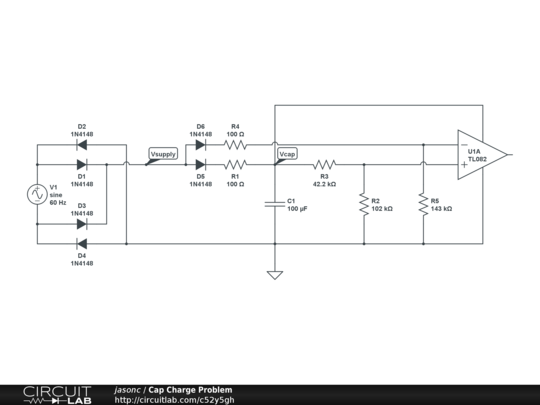
I have this circuit that I designed in CircuitLab that works as expected -- capacitor C1 charges to 24V (minus rectifier+D5+R1 voltage drop):


Plot:

download (1).png

In PSpice (orcad 16) the circuit behaves differently and C1 charges to about 31.5V despite a 24V source:

mh9374.png


Plot:

capchargeproblemplot.png

Why is this happening?

J
 
Last edited:

As you know peak voltage produce by your supply is : Vp= 1.414 Vrms - (2*0.7+0.7) = 31.836 and you have a resistor and etc.
 

As you know peak voltage produce by your supply is : Vp= 1.414 Vrms - (2*0.7+0.7) = 31.836 and you have a resistor and etc.

Thanks, but the peak voltage is 24V; the source is a 24Vpp sine wave and the plot verifies that the peak is indeed 24. I also noticed that the voltage in pspice is ~24/.707 and I think this is weird, but unless I am misreading something the source should be and appears to be 24V peak.
 
Last edited:

Try removing the opamp. Also, are both simulations using the same opamp model.

Keith
 

Try removing the opamp. Also, are both simulations using the same opamp model.

Thanks. I added this to my previous post at the same time you posted, so not sure if you saw it so I'll put it here instead, but I wrote:

me said:
Also I noticed that it does not happen if I disconnect the op amp supply connection.

I added a third diode parallel to D5/D6, connected it to another 100u capacitor to ground, and ran the op amp v+ off of that instead, and that change made C1 charge to the expected 24V but the new capacitor supplying the op amp slowly charged to nearly 280V! So I think the 24/.707 thing is sort of a red herring.

But yeah it has something to do with the op amp. Both simulations are using a TL082 but maybe CircuitLab uses a simpler model? I haven't tried it in real life so I don't know what the behavior *should* be.

It also stops overcharging if I disconnect either of the op amp inputs.

I will try to come up with a simpler test circuit in orcad.

BTW as for the supply:capacitor ratio being 0.707, turns out that's actually dependent on the R2/R3 ratio (R2/R2+R3=0.707, that's part of my design, I forgot). If I set R2 = R3 it actually charges to just under 48V (24 * 2). I don't know why. I'll test more...

- - - Updated - - -

I reduced the test circuit to this:

2s6nioh.png


Here is the plot:

2e0lc3b.png


The op amp currents seem reasonable but the voltage is pulled up to ~124V. The voltage depends on the value of R1 which seems to imply the op amp supply pins becoming something of a constant current source? But there's a cap on the voltage. Here is plot of the voltage vs R1:

34sp6bn.png


Removing the diode stops the effect. Also, it only happens if the + input is a higher voltage than the - input (using voltage dividers for the inputs still shows the behavior as long as + is higher than -, although the voltage also seems to depend on the +/- input difference).

:-?
 

In simple words, it's the result of using an OP macro model for cases that it isn't designed for. If you review the subcircuit, you'll notice, that it has a "hidden" ground node connection, which already implies incorrect simulation of the supply node behaviour.

Code:
*-----------------------------------------------------------------------------
* connections:   non-inverting input
*                | inverting input
*                | | positive power supply
*                | | | negative power supply
*                | | | | output
*                | | | | |
.subckt TL082    1 2 3 4 5
*
  c1   11 12 2.412E-12
  c2    6  7 18.00E-12
  css  10 99 5.400E-12
  dc    5 53 dy
  de   54  5 dy
  dlp  90 91 dx
  dln  92 90 dx
  dp    4  3 dx
  egnd 99  0 poly(2),(3,0),(4,0) 0 .5 .5
  fb    7 99 poly(5) vb vc ve vlp vln 0 3.467E6 -1E3 1E3 3E6 -3E6
  ga    6  0 11 12 339.3E-6
  gcm   0  6 10 99 17.01E-9
  iss  10  4 dc 234.0E-6
  hlim 90  0 vlim 1K
  j1   11  2 10 jx
  j2   12  1 10 jx
  r2    6  9 100.0E3
  rd1   3 11 2.947E3
  rd2   3 12 2.947E3
  ro1   8  5 50
  ro2   7 99 170
  rp    3  4 20.00E3
  rss  10 99 854.7E3
  vb    9  0 dc 0
  vc    3 53 dc 1.500
  ve   54  4 dc 1.500
  vlim  7  8 dc 0
  vlp  91  0 dc 50
  vln   0 92 dc 50
.model dx D(Is=800.0E-18 Rs=1)
.model dy D(Is=800.00E-18 Rs=1m Cjo=10p)
.model jx NJF(Is=2.500E-12 Beta=984.2E-6 Vto=-1)
.ends

P.S.: Did you try TL082/301/TI instead? The official TI model seems to avoid the reported effect.
 
Last edited:
  • Like
Reactions: jasonc2

    jasonc2

    Points: 2
    Helpful Answer Positive Rating
In simple words, it's the result of using an OP macro model for cases that it isn't designed for. If you review the subcircuit, you'll notice, that it has a "hidden" ground node connection, which already implies incorrect simulation of the supply node behaviour.

Thanks. I don't know enough about pspice models to identify problems like that. It actually still has the effect in the following circuit, which is disappointing because running an op-amp off halfwave -> rectifier -> filter supply doesn't really strike me as a case that the model "isn't designed for":

2wfjp85.png


Green probe: 235.99V (should settle at ~10V)
Red probe: ~235V (Should be < 10V)
Blue probe: 24V (should settle at ~5V)

In fact, in general, it fails if the op-amp's V+ and In+ are on the same side of the same diode, and In+ > In-.

2ld92x2.png


Green probe @ 110.182V (should be ~10V)
Red probe @ 109.504V (should be <10V)
Blue probe @ 24V (should be ~5V)

That circuit works fine without the diode or with the diode in the supply line but on the right side of R1. It fails when the op amp V+ and In+ are on the same side of the same diode and In+ > In-.

P.S.: Did you try TL082/301/TI instead? The official TI model seems to avoid the reported effect.

That's the problem! I was using the one from opamp.olb. The TI one works perfectly. Thanks!! That's disturbing though, I wonder how many other broken models came with PSpice? :sad:

But it's working now and I can move on with my life. Thanks again.
 
Last edited:

That's disturbing though, I wonder how many other broken models came with PSpice?
Unfortunately I don't know. You should be watchful and always check the plausibility of simulation results.

The present case is a very obvious case of a "broken" model. More generally, PSpice models don't represent all aspects of a device, at best it's clearly stated in related comments which properties are covered and which aren't, often restrictions aren't mentioned at all.

If you check the currents of individual TL082/301/TI terminals, you'll notice that they still don't sum to zero, as expected. Also this model has a hidden ground node and is not designed to model supply currents exactly, although it avoids the absurd behaviour of the generic TL082 model.

I agree that it's disappointing.

Depending on the simulation objectives you need to design your own functional models, or try to find better manufacturer models.
 
  • Like
Reactions: jasonc2

    jasonc2

    Points: 2
    Helpful Answer Positive Rating
Status
Not open for further replies.

Part and Inventory Search

Welcome to EDABoard.com

Sponsor

Back
Top