IC_fly
Newbie level 4
Hi!Did anyone done LDO VCCS compensation? I did a LDO VCCS compensation, through the voltage-controlled current source to introduce a zero point to elimanate the second main pole. but I have a question, is this VCCS output between access R1,R2 will affect the static working point? as shown in Figure 1 NETF points on a current path,
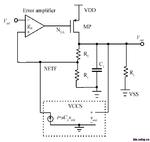
Figure 1
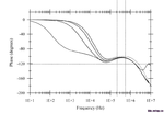
Figure 2
This can provide exchange of small signal current, but there is some static circuit outflow or inflow, affect the output precision LDO, I do not know how to fix it, I feel hard for in the VCCS control circuit to reduce the affect to the Vout, if current mirror and current sources of pipes in Figure 3 are 1:5, is part of the static current branch flowing into R1, R2.
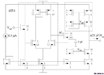
Figure 3
Then I think about VCCS is compensation capacitor of evolution and compensation capacitors are not production or absorption of quiescent current, however voltage-controlled current source may produce static electricity. And the bias current is random, deviation of temperature change as technology changes may make great effect on Vout (when T drift, PSR is bad). I have not classmate who did this LDO compensation around, so I don’t know what to do. Hope someone can help me about the experience.
with my great appreciation.

Figure 1

Figure 2
This can provide exchange of small signal current, but there is some static circuit outflow or inflow, affect the output precision LDO, I do not know how to fix it, I feel hard for in the VCCS control circuit to reduce the affect to the Vout, if current mirror and current sources of pipes in Figure 3 are 1:5, is part of the static current branch flowing into R1, R2.

Figure 3
Then I think about VCCS is compensation capacitor of evolution and compensation capacitors are not production or absorption of quiescent current, however voltage-controlled current source may produce static electricity. And the bias current is random, deviation of temperature change as technology changes may make great effect on Vout (when T drift, PSR is bad). I have not classmate who did this LDO compensation around, so I don’t know what to do. Hope someone can help me about the experience.
with my great appreciation.