Continue to Site

Welcome to EDAboard.com

Welcome to our site! EDAboard.com is an international Electronics Discussion Forum focused on EDA software, circuits, schematics, books, theory, papers, asic, pld, 8051, DSP, Network, RF, Analog Design, PCB, Service Manuals... and a whole lot more! To participate you need to register. Registration is free. Click here to register now.

Why Clock gating cells are added in a Design and how to handle during sca stitching

Status
Not open for further replies.

kothandapani

Junior Member level 3
Joined
Apr 16, 2012
Messages
30
Helped
2
Reputation
4
Reaction score
1
Trophy points
1,288
Location
Chennai
Activity points
1,501
Hi,

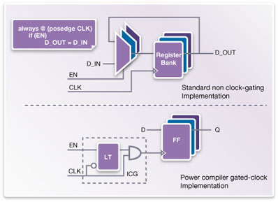
Why the Clock gating cells are added in a Design ?

As per I know the clock gating cells are added during 1. RTL stage of design and 2. During the Synthesis stage of design

1. How it will be desided to add clock gating cells durin RTl stage and where exactly it will be added in a design?

2. Who will be desided to add the clock gating cells during Synthesis and what basis it will be added during synthesis?

3. In the core netlist (before scan inserted netlist) all the clock gating cells are added and then how these are handeled during scan stiching?
 

Clock gating cells are added in the cases where you want to "swtich off" a whole clock domain (example in stand-by mode).
 

Hi ranger01,
Thanks for your updates. Also I have seen in one of the site concepts on clock gating cells,

Clock-Gating Concepts:
Figure 1 shows two circuits – one with and one without clock gating. A synchronized enable condition allows the register bank to receive either new data from D_IN, or recycled data, depending on the condition of the enable line. But in each of these conditions, the clock continues to toggle the register every time, which dissipates dynamic power. When clock gating is added, if the enable condition is not on, then the register bank is not clocked, which saves power.
The clock-gating cell shown in Figure 1 is an integrated clock-gating (ICG) cell. Compared with using discrete AND gates, ICG cells save power are more area-efficient and are less likely to cause clock-skew problems.

42_1338289374.jpg


During synthesis stage on what basis it will be added do we give any power constrains ?
Who will control the EN pin of these clock gating cells added during synthesis?
 

Hi,
Anyone please clarify above questions.

Also have another doubt here!!! what is the difference between power domain and volatage domain ?
 

In order to know how to addd. first it is very important to know "where to add". The chip/top level design guy who have the complete visibility of the chip will decide which logic is gonna use when and which logic block is not gonna use. Thus, the rtl is written with respect to this. After getting this informations. There is a tool called power compiler which takes your tech lib as well as the design plus constraints and add the CGC cells (Clock Gating Cells).

In order to use clock gating your Tech lib must have Power switches which is then use for the clock gating logics. Well, as far as your Power domain and Voltage domain questions is concerned. We have 3 types of libs which we use viz RVT-HVT-LVT. These libs are used as per the requirements. These all will tell your volatages used to model the libraries and should be used according to the rerquirement of the design.

Cheers
 

1. How it will be desided to add clock gating cells durin RTl stage and where exactly it will be added in a design?
During Architecture levek design we decide if is power critical design we add in RTL

2. Who will be decided to add the clock gating cells during Synthesis and what basis it will be added during synthesis?
Once you decided at RTL stage, let synthesis run do its best.

3. In the core netlist (before scan inserted netlist) all the clock gating cells are added and then how these are handeled during scan stiching?
While inserting the clock gating we need to mention test enable also.
 

Hi dftrtl,
Thanks for your clarifications. Now I understood the case of clock gating handled in the scan point 3.

One more question on the clock gating cells.

Consider a design, in RTL that doen't have any clock gating cells added. For that design after synthesis will it get added with clock gating cells or not? If added means on what basis will it add.
 

You have a option in synthesis to mention whether to insert clock gating or not. If you do not enable that option it will not insert any clock gating.
 

Hi Kothandapani,

The concept of clock gating is very simple. When you have a block in your architecture, which will not be used for certain amount of clock cycles, then it is wise to switch it off right? It is the basis of clock gating. ie. Low power design methodology. Now, coming to your question, we have 3 types of clock gating namely: Architecture level, comb. clock gating and sequential clock gating.

Now Architectural Clock gating is the one that our friends have described above: that the top level designer will decide for RTL coding of clock gating. Which answers your Q1.

Now your Q2 is based on Comb. Clock gating. The basis of comb. clock gating is also simple. Similar to the fact that a block can be switched off when idle can be applied to register(or flop) level. When synthesizing, the synthesis engg. will give a command called, insert clock_gating, whereby your synthesizer will automatically substitute ICG cell before "all" possible flops that can be clock gated if ICG's are available in your .lib file.

So, whether clock gating is done on RTL level or not, it is employed during synthesis of the design.

Regarding Seq. Clock gating, i dont think it is available in the tools and not necessary to discuss here. Details on this can be obtained by Googling :)

Hi Friends,

Feel free to correct me if i had gone wrong in any of my points.
 

Ok. So for a design if we enable the synth. engine to put clock gating cells on specific instances or it will read the functionality of the design and based on that it will add the clock gating cells.
 

Depends on the options you mention during synthesis Area/Effort/Power.
 

Ok. Is this my understanding is correct, It is like,

if say AREA: then it will not put any clock gating cells.
if say POWER then it will read the functionality and then it splits the design in to different power domains and put the clock gating cells. Say dom1 and dom2.
 

NO i am afraid you are wrong. A synthesizer can't read and understand the functionality and then insert clock gating cell. If a register has an enable signal, then it will map the ICG cell before the register's clock input and connect the enable condition with the ICG's en signal(it will be an AND gate with clk as one input and en as another) and will achieve clock gating.

Dftrtl tried to convey that during opt for AREA you wont use insert clock_gating command, if you do the synthesizer WILL insert ICG.
 

Thanks Sakthikumaran,
Ok. If the flop is with enable + the synth engine "enabled with" POWER then it will look for adding the clock gating cells on that particular clock tree.
But if the flop is with enable + synth engine "not enabled" POWER then it will not add any clock gating cells on that particular clock tree. Are these correct.
 

See i think you are confusing with OPT techniques and command. Their is nothing like a switch which controls optimization for area/power/speed. They are just scripts written by Synthesis guy. Here when the synthesis is meant for low power then automatically he will instruct the tool to insert clock gating cells. When his intension is for reducing area he may/maynt ask the tool to insert clock gating. So please dont confuse between process and commands. It all lies in the hands of engineer and his requirement.
 

Hi Sakthikumaran,
Ok it's all about how the design has to be optimized.
Thanks for all your clarifications. If possible any useful link or docs please point me in this post.
 

Status
Not open for further replies.

Part and Inventory Search

Welcome to EDABoard.com

Sponsor

Back
Top