Continue to Site

Welcome to EDAboard.com

Welcome to our site! EDAboard.com is an international Electronics Discussion Forum focused on EDA software, circuits, schematics, books, theory, papers, asic, pld, 8051, DSP, Network, RF, Analog Design, PCB, Service Manuals... and a whole lot more! To participate you need to register. Registration is free. Click here to register now.

how to size transistors in inverters for a particular load

Status
Not open for further replies.

VishwanathAmbli

Member level 1
Joined
May 23, 2012
Messages
33
Helped
4
Reputation
8
Reaction score
4
Trophy points
1,288
Activity points
1,466
hello,
I want to design inverter with load current 10uA for 50 ohm load.

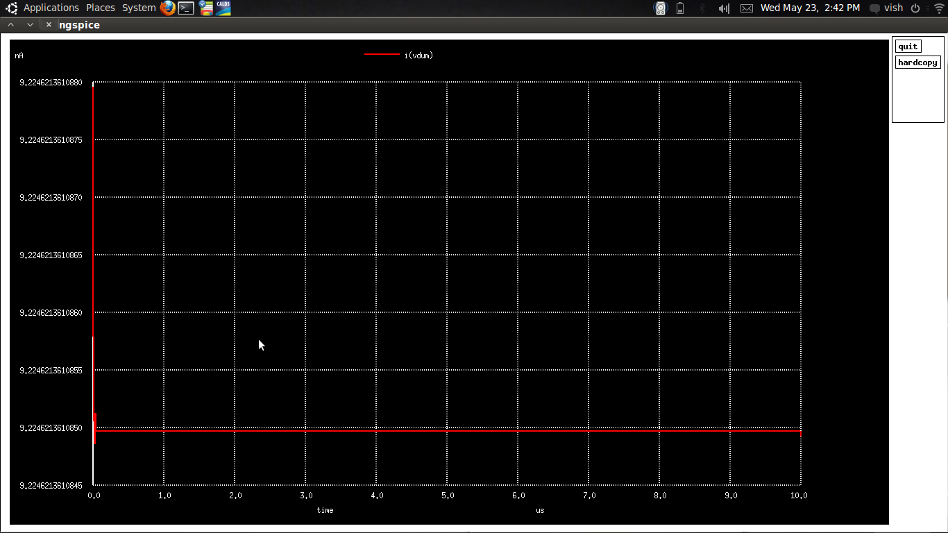
I have calculated output voltage as vout= Iload * RL and its 50x10u wch gives 0.5mV. substituting this valve in equation in the current equation of nmos and pmos equations i could get a relation between wp/wn and input voltage Vg.i simulated the same in spice but the values didn't match. i have attached here the simulated current value.. its too less than expected.
help me figure out wats wrong.


hi vishwanath,

you need to first determine what specific current you want in the inverter MOS. You can refer the pdf i am attaching here for refrence..
no matter wht model u are using for the simulations atleast this method will help u arrive at the near conclusion .
 

Attachments

  • HChible_PHD_Thesis.pdf
    210.4 KB · Views: 162
Capacitive load or resistive.
if capacitive;
Tech > 130 nm assume triode load eqn for PMOS and calculate (W/L) for amount of current needed to charge Cload to VDD.

Tech <= 130 nm
Use eqn given by baker for short channel mosfets.
 

thnx..
I ll go thru des methods n come back if drs any prob...

---------- Post added at 19:52 ---------- Previous post was at 19:51 ----------

thnx..
I ll go thru des methods n come back if drs any prob...

---------- Post added at 21:02 ---------- Previous post was at 19:52 ----------

hello,

I am reading the pdf u sent.. I know VTH0 is the threshold voltage, but wat does vt mean ... it s mentioned in weak inversion part.
 

hello muffassir,
I was wondering if u can give me some material in wch the current equation for weak inverson is derived.it wud help me.
thank u:
 

Hi Vishwanathan,

Here is below attached pdf for the derivation u can refer...


Actually what is given in the first pdf (see my first reply) the Inversion coefficient (IC)is for the EKV model of the MOS i.e. this model is valid in all regions of operaion of the MOS.


IC= Id/(Io (W/L)) for Io see the image attached its different for different technologies !

if
IC<0.1 then the MOS is in subthreshold (weak inversion) region.
0.1<IC<10 then it is in moderate inversion
IC>10 then the MOS is in strong inversion.

What u want to know is the MOS region of operation ...Id current u want in the MOS (its usually in uA when in strong inversion and nA when in weak inversion) ...and take the min value of L ..(for eg 180nm take L=0.18um )
Now u can determine the W of the transistors....U can also change the value of the L later and adjust to be able to accomodate all transistors....

This method is for EKV model of the transistors......if you are using the BSIM model then also you can apply this method to get the W/L of the transistors approximately....and can make intelligent conclusions.

Hope this helps !
 

Attachments

  • Subthreshold.pdf
    231.5 KB · Views: 122

i still didn't find the exact method t design the logical inverter...
if sm1 can help me with the steps and den how to verify the design, it wud be great.

Thnx :
 

Status
Not open for further replies.

Part and Inventory Search

Welcome to EDABoard.com

Sponsor

Back
Top