robismyname
Full Member level 6
- Joined
- Jan 17, 2008
- Messages
- 390
- Helped
- 11
- Reputation
- 22
- Reaction score
- 9
- Trophy points
- 1,298
- Location
- Central Florida
- Activity points
- 4,603
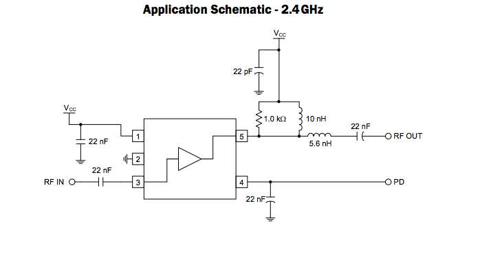
LNA Output pin.This pin is an open-collector output. It must be biased to
VCC through a choke or matching inductor. This pin is typically matched to
50Ω with a shunt bias/matching inductor and series blocking/matching
capacitor. Refer to application schematics.
Can someone tell me what the functionality of the "RF choke circuit" on pin 5 of the LNA? So pin 5 has both VCC (DC) and RF (AC)? Not sure what the description listed above really means.
please help.