Continue to Site

Welcome to EDAboard.com

Welcome to our site! EDAboard.com is an international Electronics Discussion Forum focused on EDA software, circuits, schematics, books, theory, papers, asic, pld, 8051, DSP, Network, RF, Analog Design, PCB, Service Manuals... and a whole lot more! To participate you need to register. Registration is free. Click here to register now.

[MOVED] BJT op amp design (help me plz)

Status
Not open for further replies.

farzin0123

Newbie level 5
Joined
May 19, 2012
Messages
8
Helped
0
Reputation
0
Reaction score
0
Trophy points
1,281
Activity points
1,345
hi everybody

thanks for this amazing site , im new here and sorry for my lame english

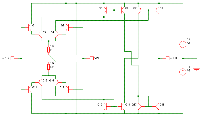
i have a project about op amp design with this Specifications : gain>100 db , phase margin>70 Deg
and rail to rail input and output .

I searched everywhere for sample of a rail to rail bjt op amp but i did'nt find ,

plz tell me your suggestions for this and Where should I start

thanks
 

Re: BJT op amp design (help me plz)

Hi. Let me see if I understand you correct. You want to build a working opamp with only bjt's and resistors?

Or, you want to build something and need to find an opamp that satisfies those criterias mentioned?
 

I assume this is really an IC design problem so I have moved it.

I am not sure how much help it will be but have a look at the LM10 - there should be some schematics in the data sheet.

Keith
 

Re: BJT op amp design (help me plz)

Hi. Let me see if I understand you correct. You want to build a working opamp with only bjt's and resistors?

Or, you want to build something and need to find an opamp that satisfies those criterias mentioned?

-------
tnx for ans...

yes i want a op amp circuit that work just with BJT Tr and resistors....l
 

I assume this is really an IC design problem so I have moved it.

I am not sure how much help it will be but have a look at the LM10 - there should be some schematics in the data sheet.

Keith

tnx bro , i look at the datasheet but it has very complex circuit
i want 3 stage ! 1 stage diffrential with folded cascode and other stage gain and outout ...

plz look at this 1.jpg

in this pic , how to bias folded cascode and convert diffrential output to single ended?
 

plz look at this....
That circuit can't swing it's output rail to rail. The LM10 doesn't have rail to rail inputs.

The circuit below has rail to rail inputs and output. The gain is too low, though. You can fix the gain and phase margin by adding a single-ended common emitter output stage with Miller compensation. I assume this is an integrated circuit design so transistor matching is no problem, but you don't want lots of resistors.

 
Last edited:
That circuit can't swing it's output rail to rail. The LM10 doesn't have rail to rail inputs.

The circuit below has rail to rail inputs and output. The gain is too low, though. You can fix the gain and phase margin by adding a single-ended common emitter output stage with Miller compensation. I assume this is an integrated circuit design so transistor matching is no problem, but you don't want lots of resistors.


Hi Godfreyl,

Could you please tell me why is Q11, Q4, Q12 and Q8 are diode connected? I know that this diode connect will reduce the gain, please tell me whats the advantage of this.
 

Yea, Got it... But diode connected transistor is connected to BJT diff pair high impedance nodes... Could you please explain why is that?
 

OK, but let me rather explain this circuit because it's a bit simpler...

Looking at the top differential pair, when VIN A is higher than VIN B, more current flows through Q3 and less current flows through Q4, so:

  • Q3 draws more current through Q5. Because the bases of Q5 and Q6 are connected together, Q6 also draws more current through Q17. Because the bases of Q17 and Q18 are connected together, Q18 also draws more current.
  • Q4 draws less current through Q7. Because the bases of Q7 and Q8 are connected together, Q8 also draws less current.
  • Q18 is drawing more current and Q8 is drawing less current, so the output is pulled down.

If you look at the bottom differential pair and follow the currents, you get the same answer; When VIN A is higher than VIN B, then the output is pulled down. When VIN B is higher than VIN A, then the output is pulled up.

If we assume that the current mirrors are perfect (output current = input current), then the collector currents of the input transistors and output transistors are related as follows:

I(Q8) = I(Q4) + I(Q13) and:
I(Q18) = I(Q14) + I(Q3)

~~~~~~~~~~~~~~~~~~~~~~~~~~~~~~~~~

Hopefully that explains the gain with a differential voltage between VIN A and VIN B.

The common mode story is interesting too, because the differential pairs are biased with resistors instead of current sources.

If the two inputs are tied together and their voltage is raised towards the positive supply voltage, The currents through Q3 and Q4 will both rise, and the currents through Q13 and Q14 will both fall. However, if you look at the equations above, you see that the currents through Q8 and Q18 both stay the same.

When the common mode input voltage is near the positive rail, the bottom differential pair is completely switched off, but the top differential pair is still working.

Similarly, when the input voltages are near the negative rail, the top differential pair is switched off, but the bottom one still works.

Because the input stages use Darlington pairs, the circuit works fine even with input voltages up to about 0.5V beyond the supply voltage.

 
A pleasure. I'm glad somebody's interested. (The OP seems to have disappeared).
 

A pleasure. I'm glad somebody's interested. (The OP seems to have disappeared).

Hey godfreyl thanks so much and others , now i want to analyze the your suggested circuit , and a question ,
in this circuit Do all Tr are biasing ? or for bias ,Should I add resistor ?
thanks..
 
Last edited:

Ah, there you are.:)
That's the complete opamp circuit, no extra resistors or other components needed.

I just used 2N2222 and 2N2904 transistors for everything in the simulation. I'm sure others would be better.

I expect you'll want to add some feedback for testing, if only to avoid DC offset.
 

Ah, there you are.:)
That's the complete opamp circuit, no extra resistors or other components needed.

I just used 2N2222 and 2N2904 transistors for everything in the simulation. I'm sure others would be better.

I expect you'll want to add some feedback for testing, if only to avoid DC offset.

im here bro :) , tnx for ans..

but I draw the circuit in your instraction by pspice but it make an error ,
ERROR -- Less than 2 connections at node N00189
ERROR -- Less than 2 connections at node N00329

Untitled.jpg
in which app you are working?

sorry for too much question :) , tnxx
 

im here bro :) , tnx for ans..

but I draw the circuit in your instraction by pspice but it make an error ,
ERROR -- Less than 2 connections at node N00189
ERROR -- Less than 2 connections at node N00329

View attachment 74716
in which app you are working?

sorry for too much question :) , tnxx


This should be a wiring/connection error. Try adding labels to all the nodes, that way you can find out which connection is having issue.
 

in which app you are working?
I use the free version of SIMetrix-SIMPLIS. I also have LTSpice installed. It's too complicated for me, but at least I can run other peoples sims. I don't have PSpice at all.
 

An amplifier design like that will have limited output drive capability and therefore limited use in the real world. The output drive current is determined by the current in the current mirrors and is effectively a class A output stage. It may be useful as a circuit within an IC where you can keep the load resistance high, but normal opamps require a low quiescent current and high output current capability which is why class AB stages are normally used. That is why output stages (particularly rail-rail ones) end up fairly complicated. The LM10 for example has a rail-rail output and can drive >20mA while taking only 300uA quiescent current.

As Godfreyl has said, your floating node errors are simply that - unconnected nodes/nets. It is possible that a net looks connected but isn't. When you pass a wire over a junction in Pspice it will not automatically connect to it, but it will look connected. SIMetrix will automatically connect a wire that runs over a pin or junction so the problem is less likely to happen.

Keith.
 
An amplifier design like that will have limited output drive capability and therefore limited use in the real world.
Agreed. I did mention earlier that an output stage will need to be added, to improve the gain and phase margin (and as you say, the output current capability, if that's important).

I just thought it would be easier for the OP if he starts by analyzing and understanding this part first, before adding more complexity. i.e. do it one step at a time.
 

Status
Not open for further replies.

Part and Inventory Search

Welcome to EDABoard.com

Sponsor

Back
Top