Continue to Site

Welcome to EDAboard.com

Welcome to our site! EDAboard.com is an international Electronics Discussion Forum focused on EDA software, circuits, schematics, books, theory, papers, asic, pld, 8051, DSP, Network, RF, Analog Design, PCB, Service Manuals... and a whole lot more! To participate you need to register. Registration is free. Click here to register now.

What is maximum switching frequency for Cheap BJT Gate drivers?

Status
Not open for further replies.

grizedale

Advanced Member level 3
Joined
Jun 13, 2011
Messages
838
Helped
17
Reputation
34
Reaction score
17
Trophy points
1,298
Activity points
8,804
Hello,

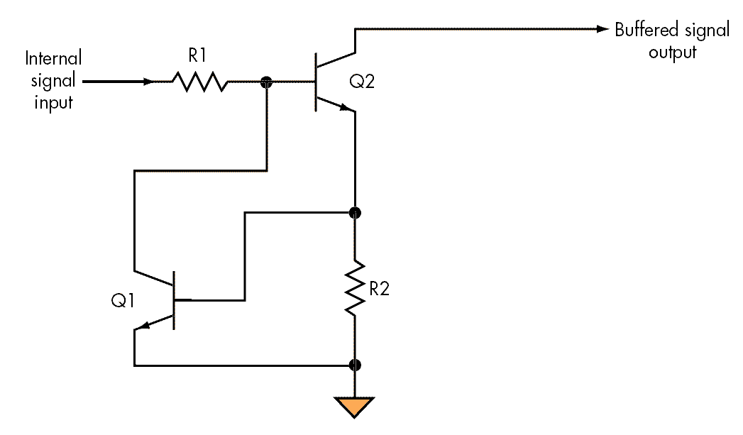
We would like to know what is the maximum switching frequency recomended for the complimentary pair BJT gate driver, driving a high side FET?

...and the BJTs being used are 2N3904

Here is the schematic of the buck LED driver using this drive method.....


R65 COMPTOR BUK.jpg
(switching frequency ends up being about 160KHz, but actually depends on the capacitor ESR)

Spec of smps:-
Led driver (425mA in each LED)
Vin = 13v


2N3904 Datasheet:-
https://www.fairchildsemi.com/ds/2N/2N3904.pdf

(we can view the gain bandwidth product and switching times etc, but they are all at particular test conditions which arent too exactly relevant)
 

Dear grizedale
Hi
It depends on ciss of your mosfet ! if you can give it high value of surge current , and discharge it's capacitor fast , there isn't any problem .
Best Wishes
Goldsmith
 
You should be able to get operation of at least 100KHz, maybe 200KHz. It will mainly depend on the PFET selection; try to get something with as low Qg and Qgd as possible.

For the gate drive circuit, eliminating R6 will help. Changing Q1 to a small FET might help turn off times too (whatever has lowest output capacitance).

And you really shouldn't have any need for the gate drive IC. The comparator should be able to drive Q1 by itself (though if Q1 is a FET I would still put a few ohms of gate resistance in).

Also what is the purpose of R5? And C2?
 
Last edited:
Thanks:

Sunnyskyguy.......linear.com stuff is too expensive for us.

Mtwieg:
R5 is simply to make up the total RDS(ON) of the fet to the same as the IRFR6215 PFET, which is used in the actual circuit.

Regarding C2, i am so relieved to hear you question it, because i have NO CLUE why they put a capacitor on a switching node....i presume its for EMC compliance, but i believe it makes EMC worse by bringing very high current spikes.
-none the less, many engineers i worked with seem to like putting ~10nF caps on switching nodes............i really really do not know why they do it........to me it is crazy.

The mosfet driver is there because the comparator shown cannot drive the bjt, and in the real circuit the comparator used is the on-chip comparator of the PIC10F204, which has more drive power, so i added the fet driver to simulate that comparator's output capability.

If i use a fet for Q1 that will mean three different transistors in the drive circuitry, and my boss will think i'm being pinnickity.

I dont feel safe about removing R6 , as this reduces shoot through currents.
--------------------

I think the 2N3906 PNP in the gate drive circuitry is going to be the biggest problem?..since PNP's are slower than NPN's.

-Anyway, when Q1 is switched off, its collector still lingers at zero volts for a few us's, which seems weird to me.

incidentally here is the ltspice simulation

Code:
Version 4
SHEET 1 2148 1224
WIRE 144 -480 32 -480
WIRE 32 -464 32 -480
WIRE 32 -368 32 -400
WIRE -1152 -240 -1152 -288
WIRE -1152 -240 -1552 -240
WIRE -272 -240 -1152 -240
WIRE -80 -240 -208 -240
WIRE 112 -240 -80 -240
WIRE 144 -240 144 -480
WIRE 144 -240 112 -240
WIRE 272 -240 144 -240
WIRE 400 -240 368 -240
WIRE 592 -240 480 -240
WIRE 656 -240 592 -240
WIRE 784 -240 736 -240
WIRE 1216 -240 784 -240
WIRE 1728 -240 1216 -240
WIRE 1216 -208 1216 -240
WIRE 1728 -208 1728 -240
WIRE -80 -192 -80 -240
WIRE -1040 -160 -1152 -160
WIRE -1040 -128 -1040 -160
WIRE 112 -112 112 -240
WIRE -272 -80 -384 -80
WIRE -80 -64 -80 -112
WIRE 48 -64 -80 -64
WIRE 1216 -64 1216 -128
WIRE 1216 -64 1072 -64
WIRE 1360 -64 1216 -64
WIRE 1728 -64 1728 -128
WIRE 1728 -64 1584 -64
WIRE 1872 -64 1728 -64
WIRE -272 -48 -272 -80
WIRE -1040 -16 -1040 -48
WIRE 1072 -16 1072 -64
WIRE 1216 -16 1216 -64
WIRE 1360 -16 1360 -64
WIRE 1584 -16 1584 -64
WIRE 1728 -16 1728 -64
WIRE 1872 -16 1872 -64
WIRE 112 16 112 -16
WIRE 288 16 288 -192
WIRE 288 16 112 16
WIRE 352 16 352 -32
WIRE 352 16 288 16
WIRE 592 16 592 -240
WIRE 672 16 592 16
WIRE 112 32 112 16
WIRE -1216 48 -1424 48
WIRE -272 80 -272 32
WIRE -144 80 -144 48
WIRE -80 80 -80 -64
WIRE -80 80 -144 80
WIRE 592 80 592 16
WIRE 672 80 672 16
WIRE 784 80 784 -240
WIRE 112 160 112 112
WIRE 1072 192 1072 48
WIRE 1216 192 1216 48
WIRE 1216 192 1072 192
WIRE 1360 192 1360 48
WIRE 1360 192 1216 192
WIRE 1584 192 1584 48
WIRE 1728 192 1728 48
WIRE 1728 192 1584 192
WIRE 1872 192 1872 48
WIRE 1872 192 1728 192
WIRE -80 208 -80 80
WIRE 48 208 -80 208
WIRE 1216 208 1216 192
WIRE 1728 208 1728 192
WIRE -1552 240 -1552 -240
WIRE 592 272 592 144
WIRE 672 272 672 144
WIRE 672 272 592 272
WIRE -768 304 -768 208
WIRE -768 304 -784 304
WIRE -656 304 -768 304
WIRE -384 304 -384 -80
WIRE -384 304 -400 304
WIRE -272 368 -272 304
WIRE -272 368 -400 368
WIRE -80 384 -80 208
WIRE -1152 400 -1152 -160
WIRE 1216 400 1216 288
WIRE 1216 400 1072 400
WIRE 1360 400 1216 400
WIRE 1728 400 1728 288
WIRE 1728 400 1584 400
WIRE 1872 400 1728 400
WIRE -1216 416 -1216 48
WIRE -1184 416 -1216 416
WIRE -1056 432 -1120 432
WIRE -784 432 -784 304
WIRE -784 432 -976 432
WIRE -272 432 -272 368
WIRE -240 432 -272 432
WIRE -144 432 -160 432
WIRE -1296 448 -1296 400
WIRE -1296 448 -1360 448
WIRE -1184 448 -1296 448
WIRE -656 496 -672 496
WIRE 1072 560 1072 400
WIRE 1216 560 1216 400
WIRE 1360 560 1360 400
WIRE 1584 560 1584 400
WIRE 1728 560 1728 400
WIRE 1872 560 1872 400
WIRE -1360 656 -1360 448
WIRE 1072 656 1072 624
WIRE 1216 656 1216 624
WIRE 1216 656 1072 656
WIRE 1360 656 1360 624
WIRE 1360 656 1216 656
WIRE 1584 656 1584 624
WIRE 1728 656 1728 624
WIRE 1728 656 1584 656
WIRE 1872 656 1872 624
WIRE 1872 656 1728 656
WIRE 1216 768 1216 656
WIRE 1488 768 1216 768
WIRE 1616 768 1488 768
WIRE 1728 768 1728 656
WIRE 1728 768 1616 768
WIRE 1488 800 1488 768
WIRE 1616 832 1616 768
WIRE 1696 832 1616 832
WIRE -1552 944 -1552 320
WIRE -1360 944 -1360 736
WIRE -1360 944 -1552 944
WIRE -1152 944 -1152 464
WIRE -1152 944 -1360 944
WIRE -672 944 -672 496
WIRE -672 944 -1152 944
WIRE -80 944 -80 480
WIRE -80 944 -672 944
WIRE 112 944 112 256
WIRE 112 944 -80 944
WIRE 592 944 592 272
WIRE 592 944 112 944
WIRE 784 944 784 144
WIRE 784 944 592 944
WIRE 976 944 784 944
WIRE 1488 944 1488 880
WIRE 1488 944 976 944
WIRE 976 1008 976 944
WIRE -1424 1136 -1424 48
WIRE 1616 1136 1616 832
WIRE 1616 1136 -1424 1136
FLAG 976 1008 0
FLAG 32 -368 0
FLAG -1040 -16 0
FLAG -272 80 0
FLAG 1696 832 rsense
FLAG -1296 400 0.6V
FLAG -768 208 Comp_out
FLAG -272 304 BJT_drive
FLAG 352 -32 PFET_gate
FLAG -144 48 BJT_bases
FLAG -1152 -288 13V
SYMBOL voltage -1552 224 R0
WINDOW 123 0 0 Left 2
WINDOW 39 24 124 Left 2
SYMATTR SpiceLine Rser=0.05
SYMATTR InstName V1
SYMATTR Value 13
SYMBOL ind 640 -224 R270
WINDOW 0 32 56 VTop 2
WINDOW 3 5 56 VBottom 2
SYMATTR InstName L1
SYMATTR Value 33µ
SYMATTR SpiceLine Rser=0.05
SYMBOL schottky 608 144 R180
WINDOW 0 24 64 Left 2
WINDOW 3 24 0 Left 2
SYMATTR InstName D1
SYMATTR Value MBRS340
SYMATTR Description Diode
SYMATTR Type diode
SYMBOL cap 768 80 R0
SYMATTR InstName C1
SYMATTR Value 100µ
SYMATTR SpiceLine Rser=0.2
SYMBOL npn -144 384 R0
SYMATTR InstName Q1
SYMATTR Value 2N3904
SYMBOL LED 1056 -16 R0
SYMATTR InstName D2
SYMATTR Value LXK2-PW14
SYMATTR Description Diode
SYMATTR Type diode
SYMBOL LED 1200 -16 R0
SYMATTR InstName D4
SYMATTR Value LXK2-PW14
SYMATTR Description Diode
SYMATTR Type diode
SYMBOL LED 1344 -16 R0
SYMATTR InstName D5
SYMATTR Value LXK2-PW14
SYMATTR Description Diode
SYMATTR Type diode
SYMBOL res 1200 192 R0
SYMATTR InstName R1
SYMATTR Value 0.22
SYMBOL res 1200 -224 R0
SYMATTR InstName R2
SYMATTR Value 0.22
SYMBOL LED 1568 -16 R0
SYMATTR InstName D8
SYMATTR Value LXK2-PW14
SYMATTR Description Diode
SYMATTR Type diode
SYMBOL LED 1712 -16 R0
SYMATTR InstName D9
SYMATTR Value LXK2-PW14
SYMATTR Description Diode
SYMATTR Type diode
SYMBOL LED 1856 -16 R0
SYMATTR InstName D10
SYMATTR Value LXK2-PW14
SYMATTR Description Diode
SYMATTR Type diode
SYMBOL res 1712 192 R0
SYMATTR InstName R3
SYMATTR Value 0.22
SYMBOL res 1712 -224 R0
SYMATTR InstName R4
SYMATTR Value 0.22
SYMBOL LED 1056 560 R0
SYMATTR InstName D17
SYMATTR Value LXK2-PW14
SYMATTR Description Diode
SYMATTR Type diode
SYMBOL LED 1200 560 R0
SYMATTR InstName D18
SYMATTR Value LXK2-PW14
SYMATTR Description Diode
SYMATTR Type diode
SYMBOL LED 1344 560 R0
SYMATTR InstName D19
SYMATTR Value LXK2-PW14
SYMATTR Description Diode
SYMATTR Type diode
SYMBOL LED 1568 560 R0
SYMATTR InstName D23
SYMATTR Value LXK2-PW14
SYMATTR Description Diode
SYMATTR Type diode
SYMBOL LED 1712 560 R0
SYMATTR InstName D24
SYMATTR Value LXK2-PW14
SYMATTR Description Diode
SYMATTR Type diode
SYMBOL LED 1856 560 R0
SYMATTR InstName D25
SYMATTR Value LXK2-PW14
SYMATTR Description Diode
SYMATTR Type diode
SYMBOL pmos 368 -192 M270
SYMATTR InstName M1
SYMATTR Value Si4425BDY
SYMBOL res 384 -224 R270
WINDOW 0 32 56 VTop 2
WINDOW 3 0 56 VBottom 2
SYMATTR InstName R5
SYMATTR Value 0.283
SYMBOL cap 656 80 R0
SYMATTR InstName C2
SYMATTR Value 10n
SYMATTR SpiceLine Rser=0.005
SYMBOL npn 48 -112 R0
SYMATTR InstName Q2
SYMATTR Value 2N3904
SYMBOL pnp 48 256 M180
SYMATTR InstName Q3
SYMATTR Value 2N3906
SYMBOL res 96 16 R0
SYMATTR InstName R6
SYMATTR Value 22r1
SYMBOL res -144 416 R90
WINDOW 0 0 56 VBottom 2
WINDOW 3 32 56 VTop 2
SYMATTR InstName R7
SYMATTR Value 1k
SYMBOL schottky -272 -224 R270
WINDOW 0 32 32 VTop 2
WINDOW 3 0 32 VBottom 2
SYMATTR InstName D26
SYMATTR Value 1N5819
SYMATTR Description Diode
SYMATTR Type diode
SYMBOL cap 16 -464 R0
SYMATTR InstName C3
SYMATTR Value 5µ
SYMATTR SpiceLine Rser=0.009
SYMBOL res -96 -208 R0
SYMATTR InstName R8
SYMATTR Value 2k2
SYMBOL res 1472 784 R0
SYMATTR InstName R9
SYMATTR Value 0.235
SYMBOL voltage -1360 640 R0
WINDOW 123 0 0 Left 2
WINDOW 39 24 124 Left 2
SYMATTR SpiceLine Rser=0.001
SYMATTR InstName V2
SYMATTR Value 0.6
SYMBOL voltage -1040 -144 R0
WINDOW 123 0 0 Left 2
WINDOW 39 24 124 Left 2
SYMATTR SpiceLine Rser=0.002
SYMATTR InstName V3
SYMATTR Value 5V1
SYMBOL PowerProducts\\LTC1693-3 -528 400 R0
SYMATTR InstName U2
SYMBOL voltage -272 -64 R0
WINDOW 123 0 0 Left 2
WINDOW 39 0 0 Left 2
SYMATTR InstName V4
SYMATTR Value 5
SYMBOL Comparators\\LT1720 -1152 368 R0
SYMATTR InstName U1
SYMBOL res -960 416 R90
WINDOW 0 0 56 VBottom 2
WINDOW 3 32 56 VTop 2
SYMATTR InstName R11
SYMATTR Value 1K
TEXT -64 1208 Left 2 !.tran 0 10 0 startup
TEXT 368 -328 Left 2 ;Si4425BDY = 64nC = Qg
 

R5 is simply to make up the total RDS(ON) of the fet to the same as the IRFR6215 PFET, which is used in the actual circuit.
That seems like a very poor choice for the application. You should be able to get something much faster for even less cost. I did a bit of searching and found this: http://search.digikey.com/us/en/products/FQD11P06TM/FQD11P06TMCT-ND/3042597
Regarding C2, i am so relieved to hear you question it, because i have NO CLUE why they put a capacitor on a switching node....i presume its for EMC compliance, but i believe it makes EMC worse by bringing very high current spikes.
-none the less, many engineers i worked with seem to like putting ~10nF caps on switching nodes............i really really do not know why they do it........to me it is crazy.
In my experience I've found that in high frequency switching supplies, the majority of near-field EMC is due to electric fields from the switching node, not B fields from the switch currents. So maybe it's to soften the E field interference at the expense of increasing B field interference, while lowering overall EMC. In any case I don't like that sort of solution, so I'd try to find a way around it (shielding).
If i use a fet for Q1 that will mean three different transistors in the drive circuitry, and my boss will think i'm being pinnickity.
Careful, he might begin to suspect you're an engineer.
I dont feel safe about removing R6 , as this reduces shoot through currents.
There's no way shoot through current can occur in that circuit. The gate drive is a class B push pull stage, not a totem pole stage. Lowering or removing R6 will increase the peak current through Q3, but that is current moving from the gate, not shoot through current.
I think the 2N3906 PNP in the gate drive circuitry is going to be the biggest problem?..since PNP's are slower than NPN's.
Nah both Q2 and Q3 never operate in saturation, so they will both be plenty fast. Q1 is definitely the bottleneck, because it has to saturate, and its output capacitance slows the rise time on the gate.
-Anyway, when Q1 is switched off, its collector still lingers at zero volts for a few us's, which seems weird to me.
Yes, this is due to the saturation of the NPN. Increasing R7 will reduce this delay. Add a parallel speed of cap to maintain fast switching. Using a FET will also eliminate that specific issue.

I made my own simplified simulations showing what I'm talking about. The circuit is duplicated, one with Q1 as a BJT, one with a NFET. In both I reduced R6 to 0.1 ohms which speeds up turn on time greatly. The one with the BJT has slightly faster turn off due to its lower Cout than the BSS123.
 

Attachments

  • grizedale PFETdrive.zip
    1.2 KB · Views: 118
Thanks for your informative simulations mtwieg.

You are right , there does appear to be no shoot through, though i wonder if the simulator is showing the ideal case, and in fact, in the real circuit, shoot-through would rear its ugly head?

In you simulations (and my one), there are in fact very short intervals where the two BJTs (NPN and PNP) in the complimentary pair are in fact saturated......however, these intervals are only around 70ns long.
-I am taking saturation as being present at any time that the Vbe>=0.7 and Vce <=0.3V. (opposite sign for PNP)

-The capacitor that you kindly placed in parallel with the base resistor of the BJT does a great job of de-saturating the BJT quickly, but pulses of current >40mA are drawn through it, from the comparator output (which is actually a pin of the microcontroller)
...the maximum current thats allowed to be drawn out of a microcontroller pin is 25mA, so we would be in danger of damaging the microcontroller with that capacitor in place.
 

Thanks for your informative simulations mtwieg.

You are right , there does appear to be no shoot through, though i wonder if the simulator is showing the ideal case, and in fact, in the real circuit, shoot-through would rear its ugly head?
No, it really can't happen. The bases of Q2 and Q3 are shorted together, so there is really no way for both of them to conduct at the same time (strictly speaking, you can get simultaneous currents in them, but that would be due to parasitic capacitance and carrier recombination, etc. Not true shoot through, and not harmful).
-The capacitor that you kindly placed in parallel with the base resistor of the BJT does a great job of de-saturating the BJT quickly, but pulses of current >40mA are drawn through it, from the comparator output (which is actually a pin of the microcontroller)
...the maximum current thats allowed to be drawn out of a microcontroller pin is 25mA, so we would be in danger of damaging the microcontroller with that capacitor in place.
That current can be lowered by just playing with the values of R7, R8, and the speed up cap. The point is you don't want the DC current into Q1 to be much more than necessary to saturate it. I tried setting R7 to 33K and the capacitor to 33pF and it works well while only drawing ~15mA peak. That will depend on the rise time of the IO pin as well.
 

BJT's like {2N3904} are not intended for high current
Ic @ 100mA, Vce=1V. ==>>>hFE min =30 and it gets worse with higher Ic. I would not use it for more than 150mA.

whereas the MOSFET{LTC1693} is capable of 1.5A pk
If you wanted to boost current, you would consider more appropriate transistors.

What is the total LED load current? Effect ESR? P/N? tolerance on V-led?

It would be much simpler to use a just this current limiter to replace the entire circuit.

Connect LED anodes to Vbat and switch the cathode string at load here.
Fig_1.gif


Control can be logic level or tied direct to Vbat.
Calculate voltage drop across transistor and choose emitter R for current level.. eg. if 1 amp choose 0R7 1W resistor
if Vce * 1amp = power dissipation .. choose proper transistor and heatsink
 
Last edited:

Thanks
Sunnyskyguy......we think we are a bit too high in power for the linear (cf switching) solution.......we are about 8 Watts total but this is from 20.4 Watts with flash duty 0.39.
Also, i hoping that since the average current in the 2N3904's is very low, that we can get away with the fact that the pulse currents being drawn through it are well above its absolute maximum current of 200mA.
Yes you are right about the low tolerance hfe value of 30 for 2n3904..........so now we have to think of a way of finding a 2n3904 that exhibits that low hfe and then test the circuit with it.
-in fact, you have brought up even more doubts to me about this circuit.

I am wondering how hfe changes with temperature...maybe we can get the low hfe value to raise its ugly head with an increase in temperature?

Mtwieg:
Thanks, though i was (mischeviously) hoping that you might say that the short duration of the (large) overcurrent means that it doesnt matter.

I believe that regarding maximum current ratings of sot23 bjts:...the main concern is the fuse-like blowing of the bond wires inside the sot23 package?...(as well as the obvious thermal situation when overcurrent is continuous)
 

> I guarantee my circuit will work for any number of LED's using PWM on R1 for high power and continuous high for < 0.5A.

It is just a matter of selection of each component. So what are the specs for each LED and your available power choices?
 

Hi,

Sunnyskyguy, Choice of toplogy i am limited to buck by employer....LED spec is as per XPEWHT.

Incidentally

I believe that the FMMT489 NPN BJT would be a better choice than the 2N3904, due to its higher hfe for high IC values. However, its "fT" value is just 150MHz wheras for the
2N3904 its 300MHz.

FMMT489 DATASHEET:
**broken link removed**

However, i presume that the lower fT isnt too relevant and that the FMMT489 would be better in every way regarding switching operation in the gate drive circuit?

Unfortunately, the FMMT489 is 100 times more expensive than the 2N3904. All of the other cheap BJTs in SOT23 package have specs like FMMT489, theres nothing say "half way" between the 2N3904 and FMMT489.
 
Last edited:

I don't think hfe is a big deal for Q1 in your circuit though. Most important is its recombination time, and its output capacitance. Recombination time very rarely specified, and is very dependent on how it's driven. But capacitance usually is given, and the 2n3904 is already quite low at 4pF. Also its price will be pretty much impossible to beat. Are you sure you need better performance than it can provide?

If you have the time, I would just buy up a variety of candidate devices with low cost and capacitance, and try them all in the real circuit. You might be surprised at what you find. For example I've found that the 2n2222 is often better than the 3904 in switching circuits, even though its specs would suggest it's slower.
 

sorry i meant using FMMT489 for Q2, and not Q1.

The second bottleneck is the 2k2 base resistor of Q2, because the 2N3904 has a low-tolerance hfe of 30, and that means that with this low hfe of 30, the maximum possible Ic is ~150mA, and thats very poor for a mosfet driver.

.....in fact its extremely poor, and would mean we would have to hunt for a BJT with that low hfe value of 30, and put it in the circuit and check that the mosfet does not overheat.

...finding a sot23 bjt with a nominal hfe of 30 will be difficult.


Also, i believe that for complementary PNP/NPN transistors used in gate driving, the most important datasheet parameter by far is high-as-possible hfe at high Ic.?

...as long as fT is above about 50MHz, then thats fine, i believe?

Also, i beleive that R6, in the place where it is, actually helps in turning off the Q3 quicker, since current flowing through R6 will deplete the Vbe voltage of the Q3 PNP.

So i agree with you that R6 does not conduct shoot thru current, but is very helpful in the place where it is.
 
Last edited:

Status
Not open for further replies.

Similar threads

Part and Inventory Search

Welcome to EDABoard.com

Sponsor

Back
Top