Welcome to our site! EDAboard.com is an international Electronics Discussion Forum focused on EDA software, circuits, schematics, books, theory, papers, asic, pld, 8051, DSP, Network, RF, Analog Design, PCB, Service Manuals... and a whole lot more! To participate you need to register. Registration is free. Click here to register now.
Hello,
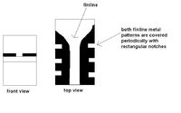
the attached picture shows a transition from finline to hollow waveguide (metallization = black).
Does anybody know the reason for these ground structures ?
Hello,
the attached picture shows a transition from finline to hollow waveguide (metallization = black).
Does anybody know the reason for these ground structures ?
@maurymw
the picture on the right side shows the transition from unilateral finline (bottom) to hollow waveguide (top).
The whole substrate is placed in parallel to the electric field maximum of TE10 mode in hollow waveguide.
This site uses cookies to help personalise content, tailor your experience and to keep you logged in if you register.
By continuing to use this site, you are consenting to our use of cookies.