Continue to Site

Welcome to EDAboard.com

Welcome to our site! EDAboard.com is an international Electronics Discussion Forum focused on EDA software, circuits, schematics, books, theory, papers, asic, pld, 8051, DSP, Network, RF, Analog Design, PCB, Service Manuals... and a whole lot more! To participate you need to register. Registration is free. Click here to register now.

Running Differential Pairs on Internal Layers

Status
Not open for further replies.

pmtwiss

Junior Member level 2
Joined
May 28, 2008
Messages
21
Helped
2
Reputation
4
Reaction score
2
Trophy points
1,283
Location
Pasadena, CA
Activity points
1,502
Hello,

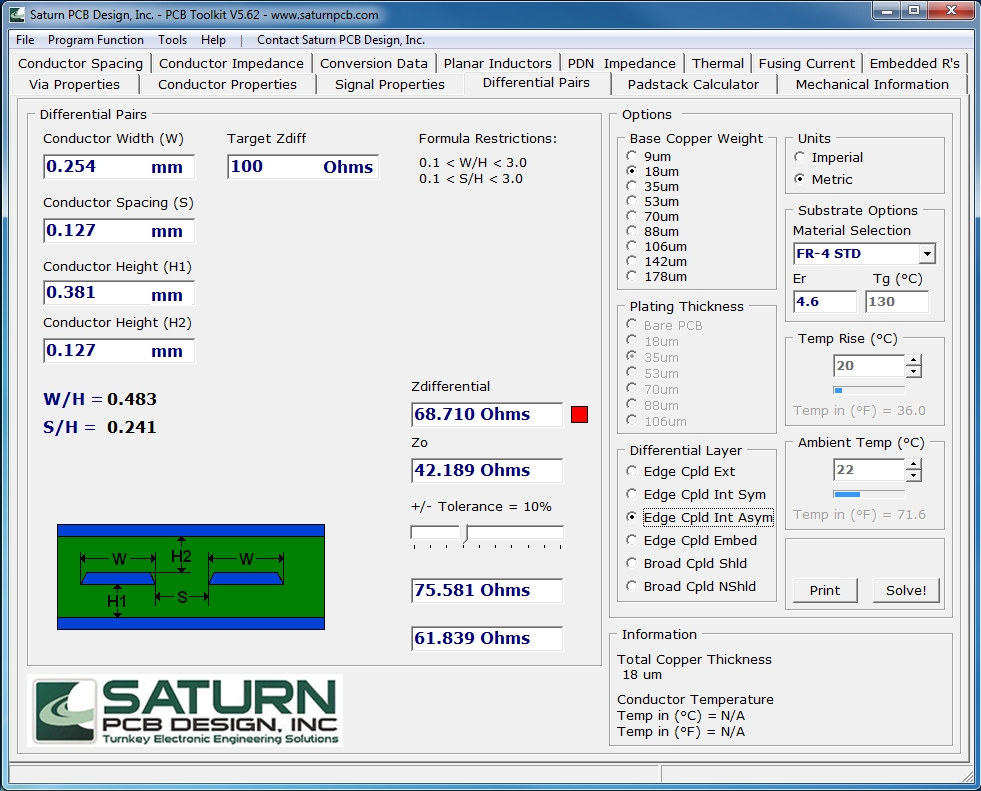
I am interested in how to find a good way to route differential pairs in the internal layers. This normally is a good idea except the fact now you have 2 reference planes, in which most tools can not calculate this b/c they are not set up to. Example is using the Saturn PCB toolkit to calculate differential pair calculations. It only give you a single reference plane. It would be nice ot be able to prdict what would happen to some accuracy when routing in internal layers as you can get good shielding this way.

Can someone add some experience or some advice or method for accurately calculating impedance on internal layers? Last time I used hyperlynx SI it couldn't do it =/

Thanx,
-Peter
 

There are calculators out there (a ton of them, just Google) - here's one... **broken link removed**
I have no idea how accurate these are, but board houses can run the calculations for you if you're with a good one.

Impedance will be less, as expected; make sure the ground planes are continuous, and when you 'launch' your differential pair into the internal signal layer, make sure to drop GND vias to stitch the planes together at this point.
One must be mindful of the return currents; try to minimize the loop created between the diff pair and the return currents that split between the two adjacent ground planes.

Regards,
Peter

Hey Pete,

Thanks for the calculator which is exactly what I wanted...showing 2 planes. But the only thing is that the plane(s) will add is shielding, and some capacitance. Keep in mind this is a differential pair and not single ended...thus there are no return currents and no loop...that is the beauty of differential, as one swings (+), the other swings (-), and in the receiver/transmitter, there is a common point. The send and return are together as one and cancel.

Thanx so much for the help man,
-Peter
 

Peter,

It is a very common misconception to think that the reference planes that bound a differential pair do not carry any currents. When you're dealing with very high speed traces, the capacitive coupling to the reference planes overshadows the adjacent differential pair. I treat each differential pair as a single trace, as far as routing is concerned, and route them with all of the normal precautions.

You're correct in thinking that by pushing the differential pair into the board, the shielding effect is helpful. If you're looking at extremely high speed stuff, consider looking at back-drilling the vias used to launch the differential pair into the board (or use blind/u vias). Sometimes transitions with stubs can leave you worse off than just completing the run point to point.

Here's two helpful articles to do with differential signaling and return currents:
http://www.signalintegrity.com/Pubs/edn/ReturnCurrentMatters.htm
http://www.signalintegrity.com/Pubs/edn/diffuturn.htm

P.S. - Remember that capacitive coupling from each trace to the environment, and even resistor tolerances (well, at these frequencies it's also the capacitive effects here) - and the inductances, are dominant factors at high frequencies. Differential signaling is never truly balanced, but we have to draw the line somewhere; and what you choose to consider in this design flow, is essentially up to your judgement as a design engineer.

Regards,
Peter
 
Last edited:

PeteEH & senilicus,

Thank you very much for your replies.

For PeteEH, what you said about the speed with regards to plane capacitance makes sense and now that I think about it I would agree...thank you for that insight..very awesome :)

For senilicus, yes you are right I just didnt see that menu...wow brain fart...thanx for the help.

Thanx for the responses guys,
-Peter
 

Again the best way to do this is to use a signal integrity verify package, and check the whole diff pair with simulation.
The number of layers and inter layer spacing will also have an effect on how closely coupled your diff pair are in relation to any adjacent planes.
 

Status
Not open for further replies.

Part and Inventory Search

Welcome to EDABoard.com

Sponsor

Back
Top