shaikss
Full Member level 4
Hi,
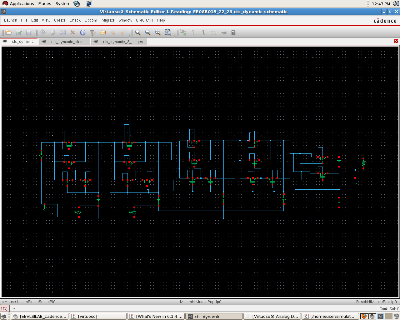
I simulated 4-stage Charge pump with dynamic CTS.
When I have given 1.8V of input voltage, I observed 7.72V as output when the NMOS bulk is connected to ground and PMOS bulk connected to drain.(Highest potential)
At the same time, I observed 8.3V as output when NMOS bulk and PMOS bulk are connected to source.
Can you please let me know while designing any circuit is it good to consider body effect or neglect the body effect?
If VSB = 0, we have neglected body effect and if VSB !=0, then body effect comes into picture.
So, whether we have to neglect it or consider it?
What may be the load current for low power applications? Load is always dynamically varying.
So, how should we know what is the load current of the system?
I may connect chargepump to some another block for example EEPROM or any digital block in my design.
What are the different parameters to consider while manipulating load current?
If I vary the load resistance,then it is equivalent to varying load current. Am I right? Please correct me if I am wrong.
Thanks,
Shaikss.