manos87
Junior Member level 1
Hello to all,
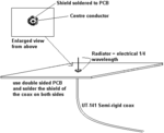
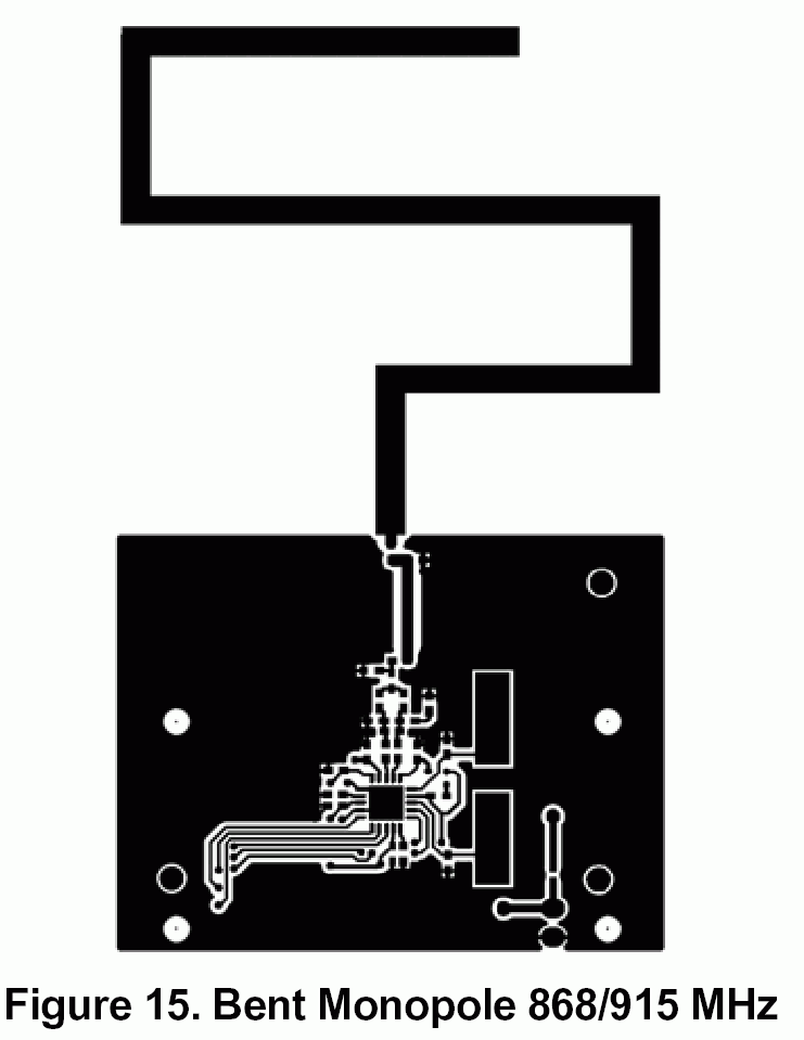
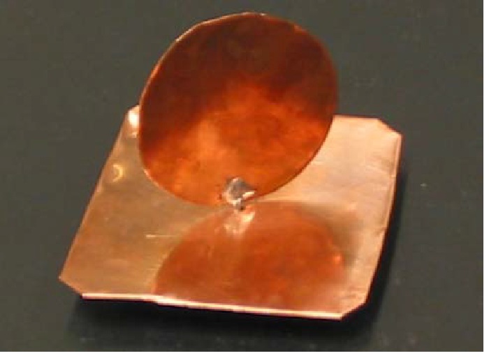
I am working on a project for channel measurements in an indoor environment and my part of this project is to design and
construt 2 quarter-wave monopoles for 2 different operating frequencies( one for 900MHz and the other for 2.4GHz).
The antennas will be made with a PCB(which is not my responsibility) and a ground plane.
I have found some information about the design but I would appreciate any additional info that you can give me.
Thanks in advance
")