Continue to Site

Welcome to EDAboard.com

Welcome to our site! EDAboard.com is an international Electronics Discussion Forum focused on EDA software, circuits, schematics, books, theory, papers, asic, pld, 8051, DSP, Network, RF, Analog Design, PCB, Service Manuals... and a whole lot more! To participate you need to register. Registration is free. Click here to register now.

LNA em_ckt_co simulation

Status
Not open for further replies.

GSarris

Member level 1
Joined
Mar 27, 2009
Messages
41
Helped
0
Reputation
0
Reaction score
0
Trophy points
1,286
Location
Netherlands
Activity points
1,616
Hello
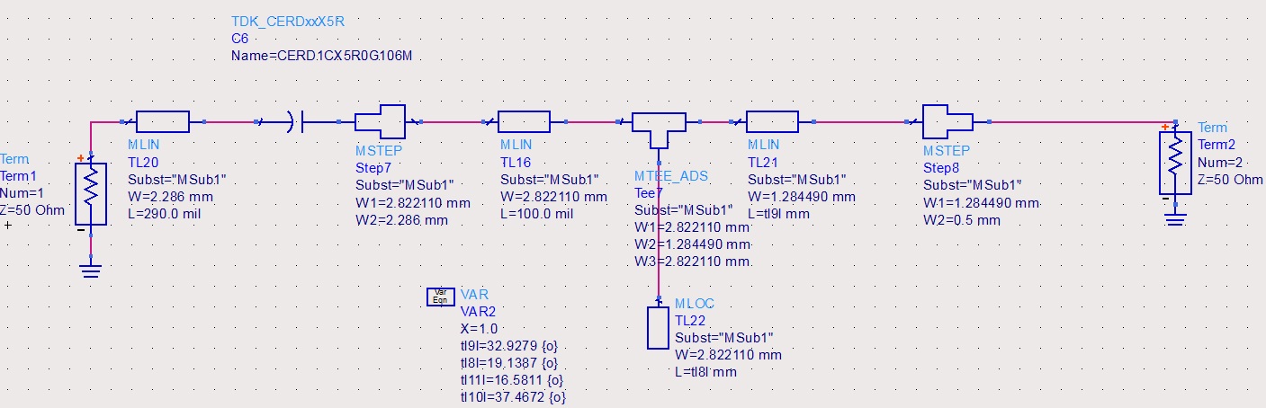
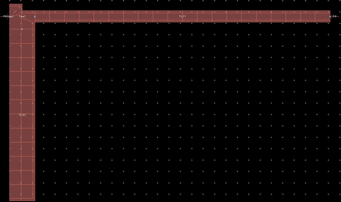
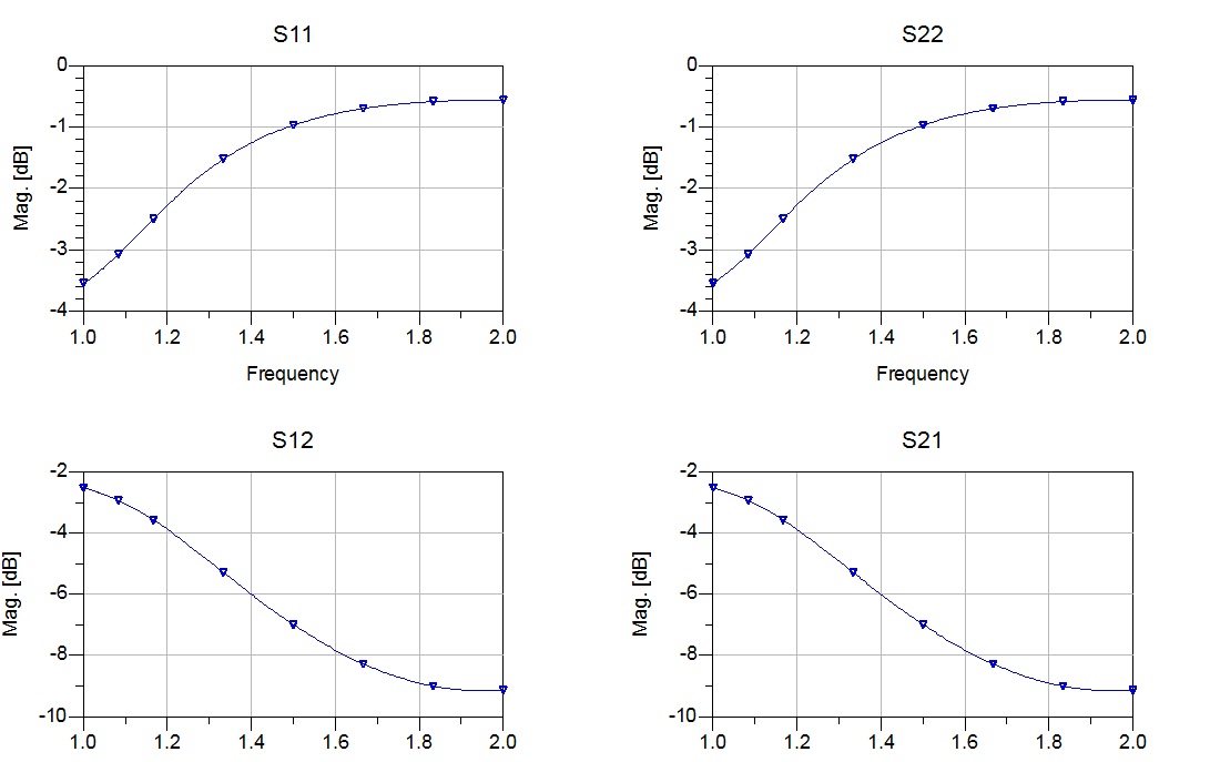
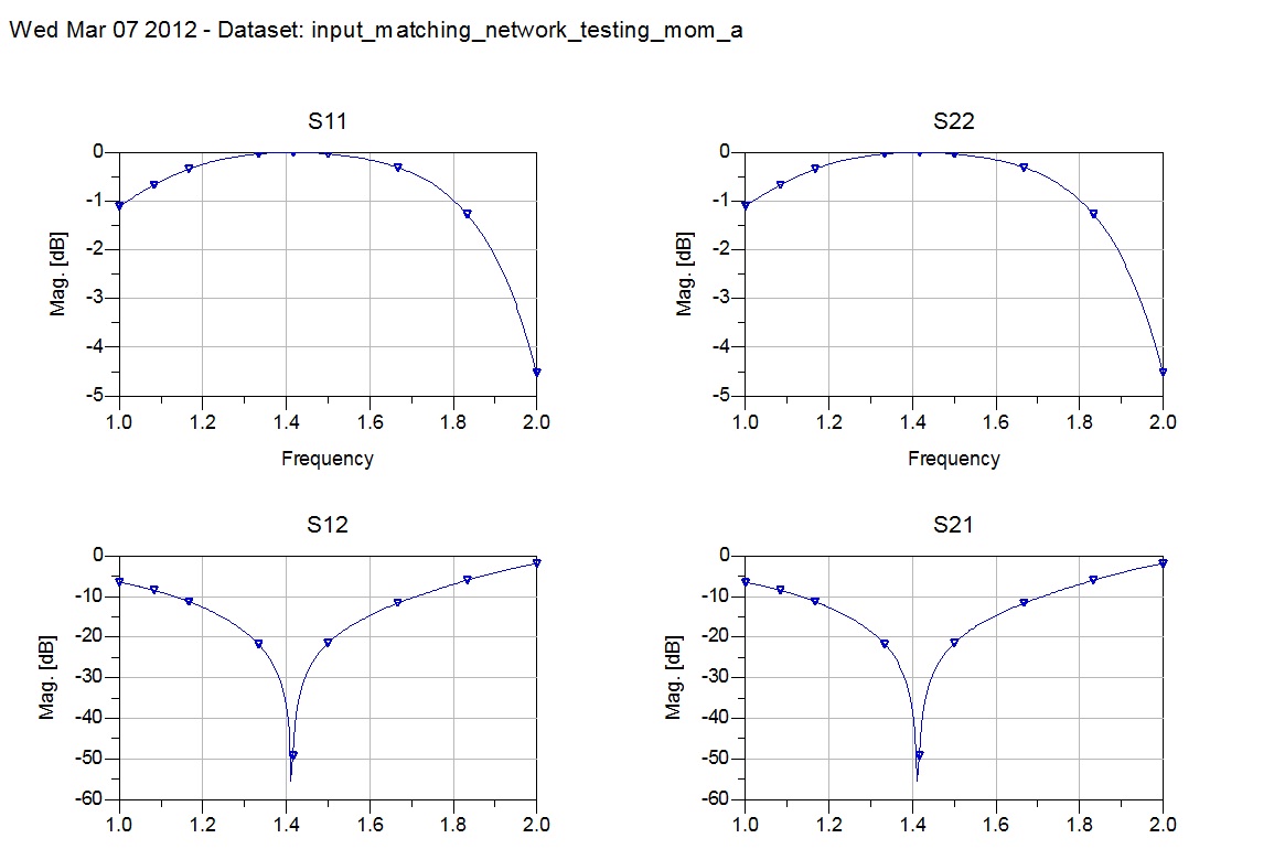
I have designed an LNA in ADS and i made the layout in order to perform the cosimulation. But results are grossly different (for example in circuit simulation the noise figure is 0.4dB while in the co simulation it tends to be 40dB and more). I suspect that i have made a serious mistake in setting up the co simulation. I followed the procedure that is described in the LNA co simulation example in the ADS examples folder but i can't find what's the problem. Can anybody help me?
Thanks in advance
Georgios Sarris
 

When you start messing with Momentum, start small and build up in small sections. I'd start with a simple trial consisting of a 1/4-wave long 50 ohm microstrip line. Make sure it looks correct (low ins loss, high return loss, etc). Then start adding your tuning artwork (open-ckt tuning stubs, etc), resim and see if it matches what you want, and repeat.

Can you attach some screenshots of your circuit, the setup screen for your layers, and the meshing configuration? (maybe even a shot of the circuit with mesh polygons turned on). The more detail, the better.... target substrate parameters (Er, height, metal thickness), freq range of operation, etc.
 
enjunear thank you for the response. i plan to do everything you say but first can i ask you a question? i have the circuit in the schematic and is performing well. what procedure do you follow to build the layout? i generate/update the layout, i connect the components in the desired fashion and afterwards i upgrade the substrate from the schematic and i am trying to set up the ground plane and the holes. Can you explain the procedure requruired to do the last 2 (ground plane and holes)?
 

enjunear thank you for the response. i plan to do everything you say but first can i ask you a question? i have the circuit in the schematic and is performing well. what procedure do you follow to build the layout? i generate/update the layout, i connect the components in the desired fashion and afterwards i upgrade the substrate from the schematic and i am trying to set up the ground plane and the holes. Can you explain the procedure requruired to do the last 2 (ground plane and holes)?

Momentum is somewhat removed from the schematic to/from layout functions (generate/update sch and/or layout). Once the metal is in the layout editor, you can think of the Momentum solver as basically importing the layout information, crunching the numbers, and spitting out a set of S parameter data.

You can define a ground plane, but the simplest way is to take advantage of the infinite ground plane that Momentum assumes by default. When you go into the Momentum layer editor, you need to define the substrate dielectric parameters. Once that's done, go to the second tab and link the layers in the stackup view with the layers from the layout editor (microstrip copper metal on cond layer, vias on via layer, etc). Select the top layer (-------) in the stackup editor, tell it to be a strip layer, then specify it to use the polygons from the cond layer.

Next, select the substrate from the stackup window, tell it to be a "via" layer, then specify it to use the polygons on the via layer; this tell Momentum to run vias through that dielectric layer, since you can have multiple dielectric layers, and vias going from layer 1 to 2, 2 to 3, 1 to 4, etc.

The bottom layer will be the infinite ground plane, so be sure you link your vias to it. One way to check that you got it correct is to layout a 50 ohm microstrip and drop a via right in the middle of it. When you run Momentum, it should look like a shorted line and some frequencies, and open at others (you basically make a shorted stub for a test). If the via isn't connected to the ground layer, then the microstrip will look like a pretty decent 50 ohm line, with a minor disturbance from an open-circuited via hanging in parallel with the 50 ohm thru line.
 
Thanks a lot enjunear! You explained it to me very well! Thanks again!
 

Hello, I have another question. I have designed my input matching network and in schematic form its response is ok. The schematic is attached. When i try to simulate it in momentum, when i simulate the part shown in the second figure (from Tee and to the right) i get a good response (3rd picture). But when i add the transmission line that is to the left of the Tee the response is bad (fourth picture). Can you please tell me what is going on?
 

Status
Not open for further replies.

Similar threads

Part and Inventory Search

Welcome to EDABoard.com

Sponsor

Back
Top