Continue to Site

Welcome to EDAboard.com

Welcome to our site! EDAboard.com is an international Electronics Discussion Forum focused on EDA software, circuits, schematics, books, theory, papers, asic, pld, 8051, DSP, Network, RF, Analog Design, PCB, Service Manuals... and a whole lot more! To participate you need to register. Registration is free. Click here to register now.

Current mode control Boost Converter

Status
Not open for further replies.

al3ko

Junior Member level 3
Joined
Apr 2, 2011
Messages
25
Helped
2
Reputation
4
Reaction score
2
Trophy points
1,283
Activity points
1,528
Dear community,

I'll have to implement a current mode control for keeping the output voltage of a boost converter constant. The converter is operating in CCM meaning the current through the inductor is never reaching 0 A.

I know the principles of current mode control with sensing the current through the switch path via a shunt/sensing resistor (or current transformer) and also the outer loop with the output voltage and the error amplifier.

The problem is, that I don't know how to design
(1) Error Amplifier compensation network for stabilizing the closed loop
(2) Find a value for the sensing resistor

I'll use the UC3842. I've also read its datasheet and I know the topologies for the slope compensation, the error amplifier etc.

But I am unable to find appropriate values for the passive components. For example:
How do I estimate the parameters for the error amplifier compensation network?

I did read books and application notes about closing the feedback loop (Fundamentals of Power Electronics, Control Loop Cookbook etc.) but they all require an exact model of the boost converter. And the model, however, is mostly given in control-to-output with the output voltage over the duty cycle (which is needed for voltage mode control).

My question to you:
How can I estimate the components for my feedback compensation network without knowing the transfer function (output voltage over inductor current)? If the transfer function is necessary, how do I obtain it easily?


I want to thank you all for your patients and help. You definitely would help me a lot because I am really lost after spending much time on reading stuff about that :(

Kindly,
al3ko

PS: The aim is to keep the output voltage constant. There won't be big load steps or any big disturbances or input changes or anything like that. So there's no need for a high bandwidth I guess.
 

First I recommend reading the following appnotes from venable tech:
https://www.venable.biz/tp-02.pdf
https://www.venable.biz/tp-05.pdf
https://www.venable.biz/tp-03.pdf
For loop compensation, you need to decide on what loop bandwidth and phase margin you need. For a given supply circuit, there are practical limitations on what can be achieved. For example boost converters operating in CCM have a right half plane zero which always limits the bandwidth to lower than that frequency.

Once you have decided on your crossover frequency and phase margin, you need to know how much phase boost you need. For that you need to know the phase and gain of your converter circuit at the crossover frequency. Measure it, model it, or calculate it. Then you design your compensation network to give an overall loop gain of 0dB and the desired phase margin at the crossover frequency. For a current mode control design, you should only really need a type II compensation network That's a quick and dirty explanation, anyways.

Also here's a pretty good app note from intersil on compensation. It suggests different pole/zero frequencies than the K factor method by venable. I've used both procedures with good results.
**broken link removed**
 
  • Like
Reactions: al3ko

    al3ko

    Points: 2
    Helpful Answer Positive Rating
Hi mtwieg,
first of all, thank you very much for your answer. And also for the links. I read them and many things (especially the ones with the stability) are more clear now. However, I am struggling with one big thing:

Once you have decided on your crossover frequency and phase margin, you need to know how much phase boost you need. For that you need to know the phase and gain of your converter circuit at the crossover frequency. Measure it, model it, or calculate it.

I've read the book "Fundamentals of Power Electronics by Robert E.". They derive the control-to-output transfer function of different converter types and I can follow them how they did it (actually I also derived the control-to-output transfer function for the boost converter by myself). Unfortunately, it is always the output voltage over the duty cycle for voltage mode control.
G(s) = v_out / d

In current mode control, I need the control-to-output transfer function with respect to my current
G(s) = v_out / i

In one of the notes you sent me, it was written that the inductor disappears in current mode control and hence there is a single roll off frequency. I really don't know how to obtain that transfer function to see the BODE plot of my converter.

Do you have a nice app or literature that explains this kind of stuff?

I only found literature explaining how to derive transfer functions for voltage mode control :/


Thank you very much
 

I've read the book "Fundamentals of Power Electronics by Robert E.". They derive the control-to-output transfer function of different converter types and I can follow them how they did it (actually I also derived the control-to-output transfer function for the boost converter by myself). Unfortunately, it is always the output voltage over the duty cycle for voltage mode control.
G(s) = v_out / d

In current mode control, I need the control-to-output transfer function with respect to my current
G(s) = v_out / i

In one of the notes you sent me, it was written that the inductor disappears in current mode control and hence there is a single roll off frequency. I really don't know how to obtain that transfer function to see the BODE plot of my converter.

Do you have a nice app or literature that explains this kind of stuff?

Thank you very much
Theoretically, the transfer function should be very similar except for having one less pole, and a different proportionality constant K. I'm not well versed enough in state space averaging to do the derivations myself, but if you can do it for voltage mode control, then it should be no more difficult for current mode control. You basically just replace your voltage controlled voltage source and inductor in the voltage control model with a voltage controlled current source in the current mode model.
 

Dear mtwieg,

thanks again for replying on my thread.

mtwieg said:
I'm not well versed enough in state space averaging to do the derivations myself, but if you can do it for voltage mode control, then it should be no more difficult for current mode control. You basically just replace your voltage controlled voltage source and inductor in the voltage control model with a voltage controlled current source in the current mode model.

I am not very versed in state space averaging, either. But I obtained the control to output transfer function of my current mode controlled boost converter and it matches very well with the literature.

The transfer function is given by

\[G(s)=\frac{v(s)}{i_c(s)}=\frac{D'R}{2}\left[\frac{1-\frac{sL}{D'^2R}}{1+\frac{sRC}{2}} \right]\]

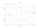
What confuses me right now, is that we only have one pole. So where will we have stability problems? It is written that we need a phase margin of around 45° away from the -180° when the gain crosses the 0dB line. But we can clearly see that we are at 270°=-90° as shown in the plot below:

bode.png

Do you understand my problem?


Kindly,
al3ko
 
Last edited:

Hi mtwieg,

I just wanted to push my thread so that you can see that I updated my post before.

Cheers,
al3ko
 

I am not very versed in state space averaging, either. But I obtained the control to output transfer function of my current mode controlled boost converter and it matches very well with the literature.

The transfer function is given by

\[G(s)=\frac{v(s)}{i_c(s)}=\frac{D'R}{2}\left[\frac{1-\frac{sL}{D'^2R}}{1+\frac{sRC}{2}} \right]\]

What confuses me right now, is that we only have one pole. So where will we have stability problems? It is written that we need a phase margin of around 45° away from the -180° when the gain crosses the 0dB line. But we can clearly see that we are at 270°=-90° as shown in the plot below:

View attachment 69755

Do you understand my problem?
I can't say whether the transfer function you give is precisely correct, but it definitely has the correct form. The bode plot clearly shows a pole, and a RHP zero.
It is written that we need a phase margin of around 45° away from the -180° when the gain crosses the 0dB line.
You're misunderstanding, I think. This applies to the transfer function of the converter, as well as the feedback, together. And the feedback loop will have its own bode plot which must be added to that of the converter. The goal is to make a feedback transfer function which has a high crossover frequency, and also a high phase margin.

Also it is wise to include the ESR of the output capacitor in the model. Depending on the capacitor type, the ESR can have important effects on the transfer function.
 

Dear mtwieg,
I can't say whether the transfer function you give is precisely correct, but it definitely has the correct form. The bode plot clearly shows a pole, and a RHP zero.
The transfer function is correct. It matches with the literature when the ESR is neglected.
You're misunderstanding, I think. This applies to the transfer function of the converter, as well as the feedback, together. And the feedback loop will have its own bode plot which must be added to that of the converter. The goal is to make a feedback transfer function which has a high crossover frequency, and also a high phase margin.
All right. Only the transfer function of my control plant is not enough. I also need the other parts of the loop. I uploaded the general schematic of my boost converter with the current mode control.

**broken link removed**


I'm using the UC3842 IC. Its datasheet can be found here:
https://www.ti.com/lit/ds/symlink/uc3842.pdf

My question is then:
What else do I need to get the open loop transfer function? In the literature, they do not include the Error Amplifier but they consider the modulator.

The open loop transfer function would then be

\[G_{OL}(s)=G_C(s)*G_{SMPS}(s)*G_{FB}(s)*G_{M}(s)\]
with
\[G_{C}(s):\] Transfer Function of Compensator to be obtained
\[G_{SMPS}(s):\] Transfer Function of Boost Converter. This one is already known
\[G_{FB}(s):\] Transfer Function of Voltage divider at the output. This is just a regular gain without any poles or zeros
\[G_{M}(s):\] Transfer Function of Modulator. Unknown as well

Do you agree so far?
The gain of the voltage divider is no problem. The datasheet of my UC3842 says:
"Comparator gain is defined as \[A_V=\frac{\Delta~V~Output~Compensation}{\Delta~V~Current~Sense~Input}\]"
The delta V of my current sense input shouldn't be any problem. I'll have to choose a resistor value that scales the current to a reasonable voltage that will be compared to the negative input of my comparator, which is by looking in the datasheet 1V.
UC3842.PNG

But how do I obtain output of the compensation network without having chosen the compensation network yet?

Too many unknowns in my design process :D

Thank you very much.

Kindly,
al3ko
 
Last edited:

The open loop transfer function would then be

\[G_{OL}(s)=G_C(s)*G_{SMPS}(s)*G_{FB}(s)*G_{M}(s)\]
with
\[G_{C}(s):\] Transfer Function of Compensator to be obtained
\[G_{SMPS}(s):\] Transfer Function of Boost Converter. This one is already known
\[G_{FB}(s):\] Transfer Function of Voltage divider at the output. This is just a regular gain without any poles or zeros
\[G_{M}(s):\] Transfer Function of Modulator. Unknown as well

Do you agree so far?
Yes, except for one thing. You can't really treat the gain of the output divider and the error amplifier compensation network as two independent systems, since they will load each other and thus interact. That is, unless you have a tranconductance error amp (you don't) or you put a buffer amp between the output of the divider and the input of the compensation network. Unless you do that you have to lump those two together into one transfer function.
But how do I obtain output of the compensation network without having chosen the compensation network yet?

Too many unknowns in my design process :D
Well, that's the fun part. There is no one right way to do it, though there are a lot of generalized approaches (like the K factor method given in one of the documents I linked).

As I said before, first you want to look at the open loop transfer function of the converter and select a reasonable desired crossover frequency and phase margin. From that, you look at the bode plot of the converter and calculate how much phase boost the compensation needs to provide to achieve that phase margin at the crossover frequency. Based on that you'll choose an compensation network type (for a CMC design a type II is almost always sufficient), and place its poles and zeros to give the desired phase boost. Then you scale the gain of the feedback network so that your crossover frequency falls where you want it.
 

Dear mtwieg,

I think I finished the compensator design. I decided against one of the compensation networks you sent me with your app notes. Firstly, because they are for voltage mode control so that the calculation and designs are based on the output LC filter and therefore a double pole in the transfer function. Secondly, I do not want to have a steady state error, so I just chose a PI compensator.

I managed to obtain all the transfer functions I need and also plotted the BODE diagram. With my compensator added, I increase my cross-over frequency from 50 rad/sec up to 1000 rad/sec and keep a phase margin of 120°.

I wanted to give you that feedback so that you can see my progress if interested. And also, I wanted to thank you very much for your help and your patience. You did a really great job and I appreciate it a lot.

Kindly,
al3ko
 
Last edited:

Be careful of overdoing the phase margin when designing the compensation network. At a certain point, additional phase margin will become very overdamped and the system will take a while to reach steady state. Also, if you use more phase boost than necessary you will likely sacrifice loop gain at low frequencies (important for fast response) and have extra gain above the crossover frequency (gain above fc should be low, for rejecting output ripple voltage). In general, a phase margin of 60 degrees is more than adequate, so I recommend adjusting things to give something closer to that. Basically, decrease your pole frequencies while raising the zero frequencies.
 

Thank you very much. I'll see what I can do.

Kindly,
al3ko
 

Status
Not open for further replies.

Part and Inventory Search

Welcome to EDABoard.com

Sponsor

Back
Top