Continue to Site

Welcome to EDAboard.com

Welcome to our site! EDAboard.com is an international Electronics Discussion Forum focused on EDA software, circuits, schematics, books, theory, papers, asic, pld, 8051, DSP, Network, RF, Analog Design, PCB, Service Manuals... and a whole lot more! To participate you need to register. Registration is free. Click here to register now.

Op amp circuit to drive 20uF load

Status
Not open for further replies.

ack88

Newbie level 5
Joined
Feb 22, 2012
Messages
8
Helped
0
Reputation
0
Reaction score
0
Trophy points
1,281
Activity points
1,340
Hello,
Thanks in advance for reading.
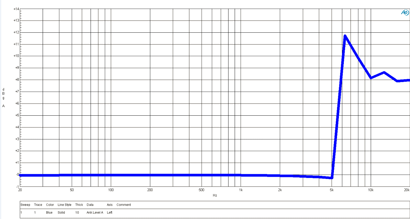
I am trying to drive a 20uF load with the opamp circuit attached .I have used AD825 op amp.Basically I am giving [Vac + (Vdc/2) ] at non inverting input and getting Vac+Vdc at output.
The output is not stable with this configuration. Do i need to put an transistor output power stage or something else for this?
Thanks
 

Attachments

  • Op amp.pdf
    145.1 KB · Views: 117

A couple of good references on the subject that might be worth reading:

"Application Note 1245 Unlimited Capacitive Load Drive Op Amp Takes Guess Work Out of Design"
**broken link removed**

Driving Capacitive Loads With Op Amps
https://ww1.microchip.com/downloads/en/appnotes/00884a.pdf


Jim
 
I've never used AD825 opamp before but I've just read its datasheet and at first glance the Figure 31 caught my attention. In that inverting topology they've measured ringing for 400pF load. Of course you have more gain but the capacitive load is also much heavier, it may become unstable. I believe you should read datasheet in detail with emphasis on phase margins for different load conditions if they are included (I haven't read the datasheet in detail.), before deciding to go for another stage.
 
  • Like
Reactions: ack88

    ack88

    Points: 2
    Helpful Answer Positive Rating
Thanks for the references it helped .
The op amp selected has unlimited capacitive loading and also it gives a good output for a limited range .
I am trying to give a 100mV -Vac at 20kHz . the slew rate for the op amp is 125V/us.
So at 20kHz i am able to give only around 19mV as input.
So any suggestions for this.
 

Your posts are raising two questions:
- conditions to achieve stability with capacitive load
- required OP parameters for 100 mV AC @ 20 kHz

I'll start with the second point. I can't follow your slew rate calculation, but you can easily calculate the required output current. I calculate about 0.25 A for 100 mV and 20 kHz, so it's obvious that a regular OP can't drive the load. A power OP, amplifier with discrete transistor booster or discrete transistor amplifier seems necessary.

The Riso principle suggested in the microcip AN can basically work. There are other circuits with better DC accuracy, but it's questionable if they offer an advantage for the present problem. The low capacitor impedance will however considerably reduce the OP GBW (gain-bandwidth product) and require an excess of bandwidth (10 - 100 MHz range) for 20 kHz signal frequency.

It should be finally mentioned, that closed loop stability with capacitive load can be better achieved with a current output amplifier (OTA) than with a voltage output one (regular OP). But there are no high current OTA chips available as far as I'm aware of. But you can implement the principle in your own amplifier design.
 
  • Like
Reactions: ack88

    ack88

    Points: 2
    Helpful Answer Positive Rating
Thanks for the reply FvM it helped a lot.
I added Riso(about 500m ohm) and checked the output it is good for about 5-7 khz but after that the same story its unstable , so to continue from here any other compensation technique with which i can deal with higher frequencies.
I have attached the response i got.
https://obrazki.elektroda.pl/91_1330395894.png
 

Analyze the loop gain and try to adjust it towards a stable roll-off. If you need a specific closed loop bandwidth as well, most likely only an amplifier with higher bandwidth can solve the problem.

For a simple hand calculation, you can assume an open loop OP output impedance of about 30 ohm, as suggested by datasheet diagram TPC 4. If you sketch the bode diagram, you see a pole/zero pair created by the output RC load (lag/lead). The unity gain transition must occur at frequencies above the zero, so with AD825, Riso must be increased above 0.5 ohm even for a unity gain buffer.

Adding an output stage may be required to drive the intended output current. But it must be a class AB stage to avoid negative loop gain effects. It's lower output impedance gives also better chances to create a stable loop.
 

The solution is accurate. However , it could help in taking a fraction of output swing and provide a bootstrap feedback to improve the transition and propagation delay.The quasicomplementary stage shall lower output current capability and boost currents needed for capacitor charging .
 

I fear, you need to show a drawing to clarify your solution.
 

Status
Not open for further replies.

Similar threads

Part and Inventory Search

Welcome to EDABoard.com

Sponsor

Back
Top