hariharan.gb
Junior Member level 1
- Joined
- Feb 2, 2012
- Messages
- 17
- Helped
- 3
- Reputation
- 6
- Reaction score
- 3
- Trophy points
- 1,283
- Location
- Bangalore, India, India
- Activity points
- 1,430
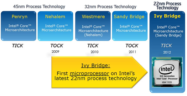
As we see in VLSI field, our technology has already reached 28nm, 18nm and so on.
With gate_size, range keep on decreasing, i believe one or the other day, it will freeze for sure.
Do researchers, targetting on pico level, pm technology like that (pico meter 10^-12)?
Is MEMS, goona do anything revolutionary here.,
please share your comments >>>>>
Hariharan B
With gate_size, range keep on decreasing, i believe one or the other day, it will freeze for sure.
Do researchers, targetting on pico level, pm technology like that (pico meter 10^-12)?
Is MEMS, goona do anything revolutionary here.,
please share your comments >>>>>
Hariharan B
")