kparrish
Junior Member level 1
i have a chip of a discrete device (connections are gnd, VS, VG, VD). i have bonded each of these pads to adapters to build a circuit, however I ran into some problems when checking the DC characteristics of the newly bonded device.
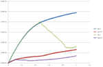
see attached image of Ids - Vds characteristics. When i measured the DC characteristics at the pads (after i had bonded the device), the characteristics were normal (blue, red). however, when i moved the probe to include the bondwire (probing at the adapter that i bonded the device to), the characteristics showed some unusual characteristics, and I'm having trouble determining the cause (green,purple). multiple devices show this sort of quality, and i tried making the measurements with increased time step to reduce any inductance effects, but the result is exactly the same. because the dc characteristics of the device are still in tact (when measured before the bondwire), i don't think the bonding damages the devices or contacts.
any thoughts on this? help is appreciated.