Continue to Site

Welcome to EDAboard.com

Welcome to our site! EDAboard.com is an international Electronics Discussion Forum focused on EDA software, circuits, schematics, books, theory, papers, asic, pld, 8051, DSP, Network, RF, Analog Design, PCB, Service Manuals... and a whole lot more! To participate you need to register. Registration is free. Click here to register now.

How to prevent gate oxide over stress on LDO pass element?

Status
Not open for further replies.

tshiu

Newbie level 6
Joined
Aug 9, 2008
Messages
14
Helped
0
Reputation
0
Reaction score
0
Trophy points
1,281
Activity points
1,379
In deep-submicrometer technologies,
the thickness of gate oxide has been scaled down to increase speed.
In the meanwhile, the breakdown voltage of gate to drain or source also decrease.
Take LDO circuits for example, in shutdown mode, Vout will discharge to 0V,
but the PMOS pass element's gate and source terminals will tight to VDD (4.5V) as the figure below,
in order to turn off pass element in shutdown mode.
This will result in overstress on Vgs and Vds.
Does cascading PMOS between Vout and pass element relax this issues or there are other better moethod?
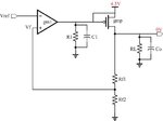
pass element gate overstress.jpg
 

If you can float the body (SOI or multi-well) then you can
stack the FETs and divide the voltage. Your Vgb and Vgs
ratings are most probably the same but Vgb is not always
called out.
 

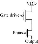
If I use the architecture as pass element (as the figure below), cascoding a core PMOS under pass element, better PSR is surely achieved.
But can it get rid of the risk of GOI damage?
pass element.jpg
 

As I understand, there is no VGS stress, but VDS stress equivalent to the supply voltage has to be tolerated which is a problem. If you use a cascode device as you have indicated, the LDO wont really be low-drop-out out in addition to causing large area and low efficiency. Moreover the VDG stress is not reduced. You could use the bottom transistor as a switch and while turning it off, tie it's source to some intermediate value (VDD/2) between supply and ground to share the VDG and VSG stresses. RON of the switch transistor would add to the drop-out voltage though.
 
  • Like
Reactions: tshiu

    tshiu

    Points: 2
    Helpful Answer Positive Rating
That scheme is fine for an LDO provided that the guard FET's leakage is
less than the control FET (Vds partitioning). It is still low dropout with
roughly 2X the on resistance (Vdrop@Iload).
 

Dick_freebird,
I hope you are referring to my scheme when you say "That scheme". Yes I agree that when the bottom transistor is used as a switch, one can keep the top transistor always ON and turn off the bottom one to turn off the LDO. You are right about that this would work as long as this transistor's VDS stress limits are beyond the supply rails.
 

Hi , Try to use NMOS across VGS of PMOS pass transistor. NMOS gate, you need not to latch to VDD. It gives better current drive but increased area.
 

I do not find any paper or reference talk about this issue on LDO pass element.
Does anyone can give me reference?
This paper discuss TDDB on nanoscale CMOS reliability, especially on startup and standby conditions.(on page 1696 and 1697)
It seems pass element in LDO will encounter this problem, too.
 

Attachments

  • [2009] Analog Circuit Design in Nanoscale CMOS Technologies.pdf
    2.4 MB · Views: 67

What is the breakdown voltage of gate oxide and drain-source?
 

Status
Not open for further replies.

Part and Inventory Search

Welcome to EDABoard.com

Sponsor

Back
Top