Continue to Site

Welcome to EDAboard.com

Welcome to our site! EDAboard.com is an international Electronics Discussion Forum focused on EDA software, circuits, schematics, books, theory, papers, asic, pld, 8051, DSP, Network, RF, Analog Design, PCB, Service Manuals... and a whole lot more! To participate you need to register. Registration is free. Click here to register now.

Clap Switch interface problem

Status
Not open for further replies.

scorrpeio

Full Member level 5
Joined
Dec 26, 2006
Messages
286
Helped
10
Reputation
20
Reaction score
9
Trophy points
1,298
Activity points
3,496
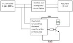
I am trying to interface the clap switch with PIC mcu.

The o/p of clap switch is 2.3-2.5V in normal state. When clap occurs the voltage changes to 6-7V.

I have to interface this switch to PIC12F IC which has max voltage level 5.5v.

I have given 5V to PIC Vcc and I have connected the clap switch to PIC using zener diode of 5.1V so that PIC is protected from over voltage.

But, in normal condition, the clap switch gives 2.3v to PIC, which PIC sometimes considers as Logic High.

Can anyone tell me what should I do to make the 2.3v at clap switch o/p as '0' V?
 

From your description, it sounds like a simple voltage divider would solve the problem. A 2:1 divider will present about 1.2V to the MCU input in the idle state and 3-3.5V when it receives a clap signal.
 
I have further analysed the circuit.
I am posting the circuit block diagram of the arrangement.

I have reaslied that the ground of Clap switch circuit and Microcontroller circuit are not common. That might be the reason why controller gets 2.3V in normal state. Am I right?

I thought to make the ground common for both the circuit. But, I dont know what will be its effect on the power supply section of both the circuits.
Please tell me, if it has any effect on the power supply sections of the individual circuits.
 

Attachments

  • ClapSwitchInterface BlockDiagram.JPG
    ClapSwitchInterface BlockDiagram.JPG
    17.2 KB · Views: 70
Last edited:

It;s hard to be perfectly sure from just a block diagram, but it seems to me that you don't have to use separate rectifier-filter supplies for the uC and the clap switch. If you need a supply higher than 5V for the clap switch circuit, you can take it from the rectifier output of the uC power supply before it passes through the 7805 regulator. Then you'll have a common ground for both circuits.
 
I have connected the ground of both the circuits.

In program I am getting the interrupt of clap switch, but the relay operates only half a way. :( :( :(

Code:
	while(1)
	{
		if(G_u1Clap1_Flag)
		{
			if(DEF_FALSE == DEF_PIN_USB_STATUS)
			{
				DEF_SET_PIN_HIGH(DEF_PIN_PC_SWITCH);
				__delay_ms(255);	//Delay of 1sec
				__delay_ms(255);
				__delay_ms(255);
				__delay_ms(255);
				DEF_SET_PIN_LOW(DEF_PIN_PC_SWITCH);
				__delay_ms(255);
				__delay_ms(255);
				__delay_ms(255);
				__delay_ms(255);
			}
			G_u1Clap1_Flag = DEF_FALSE;
		}
	}

I am turning the flag on in the ISR.
When I clap near clap switch, relay triggers but does not return back to its original position.
Ideally, as per program, there should be two sounds in relay operation....
1. Relay make and
2. Relay break

But, while operating using clap switch, I hear only one sound from relay.
Then after next clap, I hear one more sound.
Any idea?
 

Status
Not open for further replies.

Similar threads

Part and Inventory Search

Welcome to EDABoard.com

Sponsor

Back
Top