Continue to Site

Welcome to EDAboard.com

Welcome to our site! EDAboard.com is an international Electronics Discussion Forum focused on EDA software, circuits, schematics, books, theory, papers, asic, pld, 8051, DSP, Network, RF, Analog Design, PCB, Service Manuals... and a whole lot more! To participate you need to register. Registration is free. Click here to register now.

Feeding a Miccrostrip Antenna electromagnetically

Status
Not open for further replies.

antennadesign54321

Member level 1
Joined
Nov 14, 2010
Messages
34
Helped
1
Reputation
2
Reaction score
0
Trophy points
1,286
Activity points
1,530
Paper1_Page_1.jpg

Hi Everyone,

I was trying to redo the simulation of the antenna attached with this . It's mentioned on the paper that the antenna is electromagnetically coupled.

Can anyone let me know how to do feeding in this case.

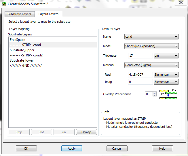
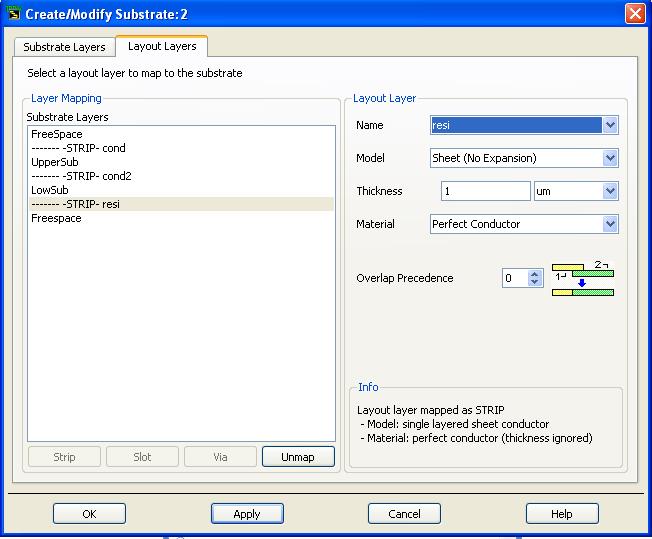
I had created a layers as such :

AIR
CON
SUBSTRATE
COND2 ( Used for Ground)
AIR


But what to do for feeding. Also in the figure it's showing 2 layers for Substrate FR4Eproxy , Why is that.


Thanks for your time.

Regards
 

Hi,

It can be seen that there are 3 metal layers: lower for grund plane, medium for feed line, and upper for patch. Between them, the 2 FR4 substrates.
The antenna is electromagnetically coupled: there is no contact with the patch. It seems that the line couples by proximity.
It is not completey clear, but it seems that the square at 45 degrees is an aperture in the patch leaving the upper FR4 visible, and behind it runs the feed line up to the metal strip that is in the upper metal layer.
What properties is supposed to have this design?
regards

Z
 
@zorro,
thanks for your response, Do you mean it will be something of this sort ?( below images
https://obrazki.elektroda.pl/41_1323712288.jpg
https://obrazki.elektroda.pl/13_1323712288.jpg

If so. How will be the ports connected,Will we need 2 ports for this case ?


Thanks for your time

---------- Post added at 18:57 ---------- Previous post was at 18:54 ----------

If the above layout is correct, Do we have to "STRIP" the Feeding Line , I dont see that button activated ?
 

I guess it is OK.
You must have a single port at the feed line (between it and the ground plane).
Note that the upper FR4 is smaller than the lower one.
For acccuracy, use a precise value of permittivity Er.
Regards

Z
 
Hi Zorro,
Thanks for your reply, I have 2 doubts :

1. Will we have to use the strip on the middle conductor ( used for feeding) , how to do that as i dont see that option activated.
2. How to connect the port to the centre feed line, as both the centre as well as top conductor are both same type of conductor, so how to we specific which conductor the port is connected to .

Can you please help me out with it, i have attached the program ( Project 1 ) w , using ads2009.

I would really appreciate your time/efforts.

Regards,
 

Attachments

  • Project1.zip
    97.1 KB · Views: 62

Hi,

I'm sorry. I can give some help about antennas, but I can't help you with ads2009.
I'm sure that in the "Electromagnetic Design and Simulation" forum you can find some experts in ADS2009.
Regards

Z
 

antennadesign54321;998250thanks for your response said:
https://obrazki.elektroda.pl/41_1323712288.jpg[/url]
https://obrazki.elektroda.pl/13_1323712288.jpg

I don't think these are correct. You stackup does not include the feedline layer in the middle.

If you have the patch layout on layer "cond" and the feedline layout on layer "cond2", you can start with an infinite ground below. The stackup definition would look like this:


Later, you can also add a finite ground layer. For this, you need another ADS drawing layer. You can use one of the predefined layers or define your own. Then, change the bottom boundray condition from /// GND /// to free space and map your finite ground layer.
 

@volker_muehlhaus , thanks for your detailed response.

I understood what you mentioned, and followed the steps, Will it be like this


Does it mean :
1. i should be linking the port1 only to Cond2
2. Once i add the Finite ground plane , i will link the port2 as a ground reference wrt port1.
3. Is it correct to select the 'resi' layer for the Ground Plane ?
4. Is it better to Conductor with Sigma rather than perfect conductor ?

thanks for your time.
Much appreciated.
 

Does it mean :
1. i should be linking the port1 only to Cond2
2. Once i add the Finite ground plane , i will link the port2 as a ground reference wrt port1.

I am not a Momentum user (use Sonnet), but from what I understand about Momentum: yes, both is correct.

3. Is it correct to select the 'resi' layer for the Ground Plane ?

The layer name is only a name, so you are free to choose what layer you want to use. Personally, I would prefer to define a new layer with a meaningful name.

4. Is it better to Conductor with Sigma rather than perfect conductor ?

It is more realistic to include the metal losses.
 

Status
Not open for further replies.

Part and Inventory Search

Welcome to EDABoard.com

Sponsor

Back
Top