Continue to Site

Welcome to EDAboard.com

Welcome to our site! EDAboard.com is an international Electronics Discussion Forum focused on EDA software, circuits, schematics, books, theory, papers, asic, pld, 8051, DSP, Network, RF, Analog Design, PCB, Service Manuals... and a whole lot more! To participate you need to register. Registration is free. Click here to register now.

design sample ana hold circuit using op-amp

Status
Not open for further replies.

fidomido

Newbie level 6
Joined
Nov 30, 2011
Messages
13
Helped
0
Reputation
0
Reaction score
0
Trophy points
1,281
Activity points
1,357
heeey


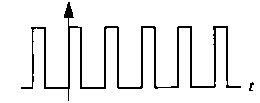
i have to design a sample and hold circuit by using this op-amp


sampling%20.jpg


my advisor confirmed this design but i have problems with the vaules so could any one here help me


thanks a lot

regards
 

The capacitor, needs to charge up via the FET switch and the output impedance of the first Op amp during the time the sample pulse exists. So if its too large it never charges to the correct value. When the sample gate is closed the capacitor then discharges through the back resistance of the FET and the input impedance of the output OP amp, so if the capacitor is too small, its voltage will decay giving a "low" value for the stored voltage.
Frank
 

thanks a lot for the explain my friend but i want values for these components or give me simple design with values to (sample and hold using op-amp)


regards
 

You cannot just ask for values!
Run simulations first.
You know fs, power supply, and input range, then you have do run sims to make sure the 1st opamp amplify the input to the desired range and filter the outofband noise. Then decide the switch and the cap to make sure it settles in less than half the clock period. Then the bandwidth and accuracy and stability of the 2nd opamp can be decided.
 

how can i run the simulation with out values !!!!!!!
 

To decide about component values, we need to know the OP and switch transistor types first. In addition, there's no particular need to give the input stage a gain > 1, it can be configured a s buffer similar to the output stage as well.

A reasonable capacitor value depends on the signal time scale, sample rate and available acquisition time.
 

ok can u give me any complete design with values ????
 

You haven't specified any performance criteria so how can anyone specify values? You need to define the range of input signal frequency and the sampling rate you want. As with any design there is not a single right answer. The sampling capacitor needs to be large enough to hold the value with minimal droop (which needs specifying) but small enough so it can be charged quickly by the preceding opamp/FET without causing instability in the opamp due to accessing capacitive load. Provided a CMOS sample buffer is used, something like 100pF might be a reasonable starting point for experimentation. You may find charge injection problems from the FET if you use a MOSFET so that may force you to increase the capacitor.

Keith
 

my advisor want a pulse ampilitude modultion by using sample and hold circuit without any special criteria , just he wants to see the circuit if it works or not
 

without any special criteria

Not particulary special, but you should at least write pulse width and period numbers to your sampling signal waveform...

86_1323618244.gif
 

"how can i run the simulation with out values !!!!!!!". Draw circuit, stick in any values, run simulation, inspect results, if not satisfactory repeat with different values. Eventually you will learn what effects what - Brilliant!
Frank
 

Status
Not open for further replies.

Similar threads

Part and Inventory Search

Welcome to EDABoard.com

Sponsor

Back
Top