Continue to Site

Welcome to EDAboard.com

Welcome to our site! EDAboard.com is an international Electronics Discussion Forum focused on EDA software, circuits, schematics, books, theory, papers, asic, pld, 8051, DSP, Network, RF, Analog Design, PCB, Service Manuals... and a whole lot more! To participate you need to register. Registration is free. Click here to register now.

[SOLVED] Gain and Phase Margin (Folded Cascode

Status
Not open for further replies.

chikaofili

Junior Member level 3
Joined
Jun 29, 2011
Messages
30
Helped
0
Reputation
0
Reaction score
0
Trophy points
1,286
Activity points
1,510
Hello,
I have an assignment for a DDA (Differential Difference Ampplifer) where
Vo= A( (Vpp-Vpn) -( Vnp - Vnn))

Hence Vo= A[(Vpp+Vnn) - (Vpn+Vnp)]

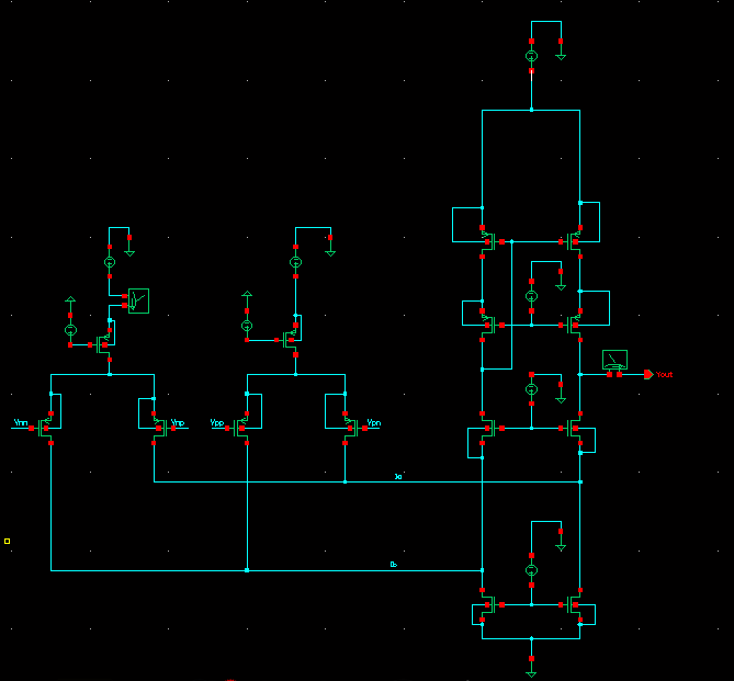
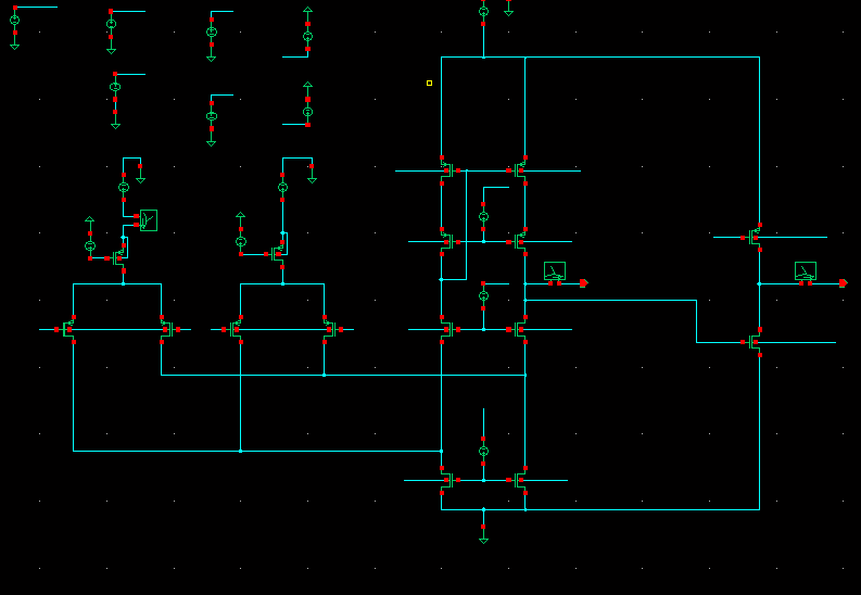
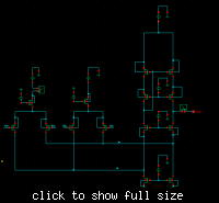
Then I have two input different stage that then add before it gets into the folded cascode stage (Hope I am making sense)


But I have the following specs
Vdd= 1.8v
Total current=150uA
Vpn:Vnn= 0- 0.9V
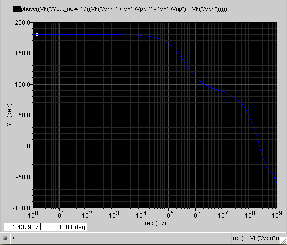
Phase Margin: >45deg
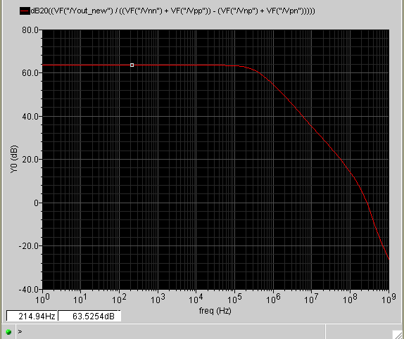
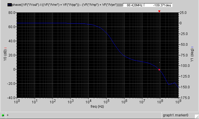
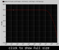
Gain: >60dB


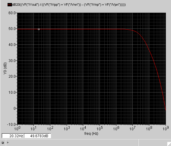
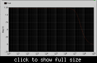
At this point, my design is embarrassing. I can only get the voltage up to 50dB.

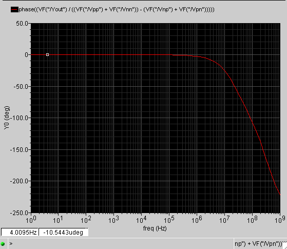
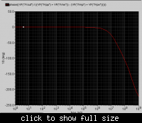
And the phase margin is worse -39deg :(

I know that the A= Gm Rout
and to improve Gm: I have to increase the W/L or/and I of the input stage
and the Rout of the differential stage.

But with the restriction of the power consumption, I am kinda at a dead end. <~ Maybe I should crank up the current and disregard the restriction?


I used the parameter sweep to get the Widths of the various pmos and nmos of the cascode stage.

How can I improve the phase margin?

Any help/suggestion will be appreciated.

Thanks

* I attached pictures


First of all, your Nmos and Pmos are connected locally within your amplifier. I would think this is a mistake because you will have to increase your area for the spacing of the Pmos in layout and you would need a triple well process for the Nmos... so I would first have all bodies of Nmos connected to ground and all Pmos bodies connected to VDD. Also this is a single stage amplifier, thus one dominate pole, so your phase margin should be 90degrees. I would think you do not have a Cap on your output, thus your output pole and current mirror poles are close ( at high frequency) and thus your PM is low. Also you don't have any spec for gain bandwidth product (GBW)? I see its around 1GHz. If a lower GBW is OK, then you can increase you min L of your output transistors to boost there impedance at the price of speed.
hope this helps
Jgk
 
Thank you so much!
I will try your suggestions now.
To be quite honest. I am pretty lost when it comes to finding the dominant pole.
Also where you suggesting i add a capacitor (Cc) at Yout? for compensation of PM? What range of values can I use? How will it affect the gain also?


Sorry I am asking quite stupid questions. I am not familiar with Compensation capacitors and all.
 

No question is a stupid question! The dominant pole should always be the output when only having a single stage amplifier or the first stage in a second or multi-stage amplifier. When adding Cload to a single stage design, you shift your dominate pole to a lower frequency which increases your PM and makes your amplifier stable. It will not affect the DC gain but will change your open loop bandwidth by lowering it. As for values, the larger the cap, the smaller the open loop bandwidth. so it all depends on what you need for a bandwidth. Try just starting with a 1pF and see what you get

jgk
 
Hello,
Thank you so much for your great help.

Without the attachment of the following transistors in (image 1). I was able to get 60db and 34deg phase margin by cranking up the length as you have advised.


But someone told me to add to those transistors for compensation (not sure why)

I was able to get the right amount of gain but my phase margin plot is weird. I though it starts at 0deg and goes down below -180deg. But it is at the positive side?? Not sure what that means.

According to the calculator on cadence. The phase margin is 168. But I feel something is wrong


---------- Post added at 22:06 ---------- Previous post was at 21:45 ----------

Is it possible to compensate it without a capacitor? like with a transistor instead
 
Last edited:

What size is your cload? If you just increase it you will see your PM increase!
 

Hi jgk2004
Were you able to meet the commom mode spec of 0-->-.9V with Pmos only input stage?
You can try reducing the parasitic cap at the folding node, which could also help in moving both the zero & the pole..
 

I am little lost with the question/statement. If your transistors PMOS have a Vth of lets guess.. 500 to 600mV and then an over drive of say 80mV...Weak inversion, that leaves you with 220mV-320mV for your tail current Vds. Since the discussed schematic is a non-cascode current mirror, you should be fine! If you cascode it, you could have both transistors have overdrives of say 100mV and still have 20 left and thats worst case!

As for the statement on reducing the parasitic at the cap node.. There has never been a spec on GBW. So since it sounds like it isn't important, just add a larger Cload! and DONE! PM goes up.. If you want to reduce the cap at the folding node, it will most-likely cost you gm since that would include decreasing the width and or length of your input pair..not good for your gain. or if you decrease the size of your transistors in your output, the Rds goes down due to short channel effects DC gain decreases as well...


Jgk
 

Thank you soooo sooo much :)... It worked!

I was able to get it to 46deg and the gain as 61dB. Its enough for now.

I removed those two transistors tho.. When I increased the lengths of my transistors for some weird reason it worked.
 

What you removed the two output transistors.. which make a second stage amplifier thsu your PM should have been very low without compensation?
Jgk
 

Hi,

So you basically removed the second stage? What is ur UGB & load cap?


jgk2004
yeah, but the process we use has an vt around 0.9v at worst corners...
 

What I meant was that i removed the extra pmos and nmos because I didnt need that much gain (just 60dB).

And then readjusted the whole circuit because I think I made a mistake in finding the working range of the system before.

Are you saying that by removing those extra transistors, my PM should have been lower?

I attached the phase diagram


when you had a 2 stage design, you need to set any one of the pole the dominant, so you need to add a compensation cap this would have lower phase margin.
without the second stage you now have a single stage system so you will have higher phase margin.
 

Status
Not open for further replies.

Part and Inventory Search

Welcome to EDABoard.com

Sponsor

Back
Top