Continue to Site

Welcome to EDAboard.com

Welcome to our site! EDAboard.com is an international Electronics Discussion Forum focused on EDA software, circuits, schematics, books, theory, papers, asic, pld, 8051, DSP, Network, RF, Analog Design, PCB, Service Manuals... and a whole lot more! To participate you need to register. Registration is free. Click here to register now.

gnd connection for jtag

Status
Not open for further replies.

spman

Advanced Member level 4
Joined
Aug 15, 2010
Messages
113
Helped
0
Reputation
0
Reaction score
0
Trophy points
1,296
Activity points
2,061
Hi,
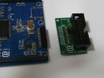
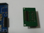
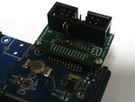
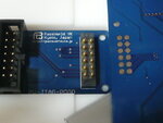
Why standard jtag connector has multiple grounds?

The grounds are clearly shorted. so i think it is ineffective to have multiple grounds and a smaller connector containing one ground is feasible.
what happens if i make small the connector in my PCB? i want to connect the programmer connector with one line of GND to the PCB.
 

spman said:
what happens if i make small the connector in my PCB? i want to connect the programmer connector with one line of GND to the PCB.

You could do that, but you need an adapter board. Please see attached picture. This is a jtag adapter for avr. In the red circle you can see the adapter board with the jtag connector on it. This is where jtag is plugged. In the blue circle you can see the part that is plugged on the board (ends as single in line). However, I don't think that it is good to use it when you are comfortable with your board space, the JTAG manufacturer gave this pinout for some reason. But when your board space is limited, then you do not have much of a choice.

JTAG adapter.JPG
 
Last edited:
  • Like
Reactions: spman

    spman

    Points: 2
    Helpful Answer Positive Rating
The multiple grounds are there for two reasons, you *might* get away with reducing them but there are risks of signal corruption:

1. they reduce the impedance between programmer and the board, this will produce a cleaner programming waveform,
2. when a ribbon cable is used it ensures alternate wires are ground so the cross-talk between signals is minimized.

Brian.

 
The multiple ground pin assignment of the shown JTAG connector is preferable for high speed operation. Signal lines are separated by ground line in the flat cable. I assume it's a standard ARM JTAG connector, it also exposes a RTCK signal that isn't generally used by all JTAG implementations.

Besides the ARM JTAG scheme, there are various vendor specific pin assignments in use, most have only 6 or 10 pins. If working at low (e.g. Wiggler) or moderate JTAG speeds, there should be no problem to use a kind of minimal JTAG interface. If you intend to use dedicated hardware debug adapters, you better stay with the original ARM interface.
 
  • Like
Reactions: spman

    spman

    Points: 2
    Helpful Answer Positive Rating
Hello!

I suppose you are looking for solutions that would allow you to use smaller
connectors than the standard bulky stuff.
As I am doing only small portable devices (which can be sometimes as small
as a regular JTAG connector), I also need smaller solutions.
Please have a look at the attached pictures.

IMG1 shows a board with a custom 12-pin single row 1.27 mm connector. As you
can see, this JTAG connector is quite thin and it saves you a lot of space compared
to the regular JTAG connector on the green adaptor board. Its height is 2.3 mm
only above the board. I have made a similar board for ARM and it also fits with
12 pins, single row.

IMG2: On the opposite side of the adaptor board, you can see the male pins.
On my first adaptor, these pins were completely out of the board, but as they
are fragile, I have put the connector a bit more inside so they are protected
by the board.

IMG3. Another advantage of a larger adaptor board beside protecting the pins
is that you can assemble the adaptor and your board with screws. therefore,
you cannot accidentally unplug it and / or bend the male pins.

IMG4. Another solution is to use no connector at all on the target board but
instead draw pads on the solder side of the target board, and fit them with
spring loaded pins. This picture shows the solder side of a board and a part
of the programming device that I have milled in an acrylic plate.

Note: All these pictures are fore MSP430 JTAG but can be adapted to any
other JTAG.

What is said in the above replies is certainly true. Having GND - sig - GND
alternating allows you to reduce cross talk between your signal lines.
In the case of this adaptor board, this is still almost true. The length of
the non-alternating connections between your 20-pin IDE cable and the
board is about 10mm, and there is no noticeable influence of noise or
crosstalk. Note that this is based on experience only. I have no means
of measuring crosstalk in my cable + adaptor assembly vs the same
cable without adaptor.

Dora.
 

Attachments

  • IMG1.JPG
    IMG1.JPG
    70.3 KB · Views: 86
  • IMG2.JPG
    IMG2.JPG
    55.8 KB · Views: 75
  • IMG3.JPG
    IMG3.JPG
    65 KB · Views: 68
  • IMG4.JPG
    IMG4.JPG
    65.9 KB · Views: 73
  • Like
Reactions: spman

    spman

    Points: 2
    Helpful Answer Positive Rating
Thanks for your attention

I have another doubt with one line of GND connection. Suppose a transport in which some signals are high and others are low. Regarding to value of signals, each side wants to sink or source current for detecting values. But there is one GND connection and in a moment it can't be a media for sinking and also sourcing. so conflict is occurred
Is it true?
 

hi

i have problems discovering jtag pins on the router board and the original single row 12 pin search took me here, besides that i could not find any information regarding this type of connector so it would be nice if someone could help me.

the board itself does not actually have a connector but only points pulled out of circuitry, i tried using standard jtag 3-5-7-9 pins but it's not working.

after found someone else with the same type of connector (too bad he hasn't provided more information) on this page https://www.mobileread.com/forums/showthread.php?t=147923 and saw he used last 3 pins i took another look at my board and here are pins 2-9 all conected to 2 elements with 101 designation on them (the one in white rectangle). for this reason i think the pins 2-9 are GND and pins 1, 10, 11, 12 should be the ones for jtag data connection but i need someone with more experience to confirm this or tell me where am i wrong if i'm mistaken.

**broken link removed**

thanks!
 

my assumption was wrong as i see on another picture i managed to find the pins are named and now it's clear the guy i mentioned in my previous post used serial connection.

but these two devices seem to be pretty much alike (ebook reader) and that's why i'm not sure if the pins are same on my router.

can anybody confirm this pinout is standard for this type of connector? also i noticed when a piece of wire just touches pin 8 without being connected elsewhere the ethernet LEDs are glowing for couple of seconds
 

Attachments

  • NetronixEB600_Serial_Port_Pinout_32MB.jpg
    NetronixEB600_Serial_Port_Pinout_32MB.jpg
    649 KB · Views: 100

Status
Not open for further replies.

Part and Inventory Search

Welcome to EDABoard.com

Sponsor

Back
Top