Continue to Site

Welcome to EDAboard.com

Welcome to our site! EDAboard.com is an international Electronics Discussion Forum focused on EDA software, circuits, schematics, books, theory, papers, asic, pld, 8051, DSP, Network, RF, Analog Design, PCB, Service Manuals... and a whole lot more! To participate you need to register. Registration is free. Click here to register now.

Help with highpower LED circuit protection

Status
Not open for further replies.

ELEFANTOMET

Junior Member level 2
Joined
Sep 26, 2011
Messages
23
Helped
0
Reputation
0
Reaction score
0
Trophy points
1,281
Activity points
1,452
LED Circuit.JPG

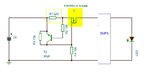
Ive been working on a solution to ensure that the SMPS for my Highpower LED, doesnt get more than 15W in a minute in case of a short.
The solution ive been working on is the one attached, using the 10R resistor, simulating a short, by connecting the 10R resistor(since theres impedance match, the power should not exceed 12V^2/10R=14.4W).
Some1 suggested me the Zener & Capacitor, because the SMPS needs 2.8A to start switching, and without theese two, it only gets 1.2A?
Can some1 explain me the function of the zener and capacitor. The way its connected here, the zener burns out and make a short, why is that?

Best regards.
 

i think a higher voltage of zener should work first try simulating and see the results
 

If i understand it correct, and im not sure i do.

If i place a 16V Zener, then i'd have a voltage drop of 8V over the first 10R. When i make a short by connecting the 2nd 10R, i'd have a voltage drop of 16V over the 2nd 10R. Thats 25W in that 2nd resistor, which is too much.
 

Better to use a current protection circuit, see for example the attached diagram.
The P MOSFET need to be mounted on a proper heatsink, short circuit current value limited by the 0.33 ohms resistor
I= 0.6V/R
 

Attachments

  • protection current.JPG
    protection current.JPG
    27.4 KB · Views: 128

Could you explain a bit more in details how the circuit works, i dont really understand it. Would be much appreciated.
 

It’s a fairly simple scheme the current limiter. Think of the current-limiting circuit as a resistor that can change its resistance. It will automatically detect the amount of current that should be flowing through and change its resistance accordingly. The incoming current first goes through a current sensor (R1) whose output signal goes to a PNP transistor. R3 and R4 form a voltage divider providing bias to T1. Initially PNP transistor T2 blocked, the transistor will remain off until its emitter to base voltage exceeds the emitter to base forward diode drop (approximately 0.6V). During normal operation (as load current is less than the limit value) the P- MOSFET should be fully on. As the load increases (load resistance decreases) a voltage drop will develop across sense resistor R1, to the point at which the current limit is reached (UR1 >0.6V), in that moment T2 open and current begins to flow out of the collector of T2 and through R4 to ground. Therefore, the total current passing through R4 increases by the amount supplied by the collector of T2. The effect of increased current through R4 is an increase in the gate voltage of T1, and therefore an increase in the VGS voltage. VGS will continue to rise until T1 will begin to shutdown, reducing the output current. Ultimately a balance will be reached as T2 supplies sufficient current to supply a VGS value that limits the output current to 2A. Series resistor only drop about 660mV @ 2A, but the P-MOSFET will get really hot under sustained 2A load.
 

Status
Not open for further replies.

Similar threads

Part and Inventory Search

Welcome to EDABoard.com

Sponsor

Back
Top