Continue to Site

Welcome to EDAboard.com

Welcome to our site! EDAboard.com is an international Electronics Discussion Forum focused on EDA software, circuits, schematics, books, theory, papers, asic, pld, 8051, DSP, Network, RF, Analog Design, PCB, Service Manuals... and a whole lot more! To participate you need to register. Registration is free. Click here to register now.

The Current ouptut 150 Amps power supply problem

Status
Not open for further replies.

Pavel1986STula

Newbie level 6
Joined
Sep 21, 2010
Messages
11
Helped
0
Reputation
0
Reaction score
0
Trophy points
1,281
Location
Russia, Tula
Activity points
1,403
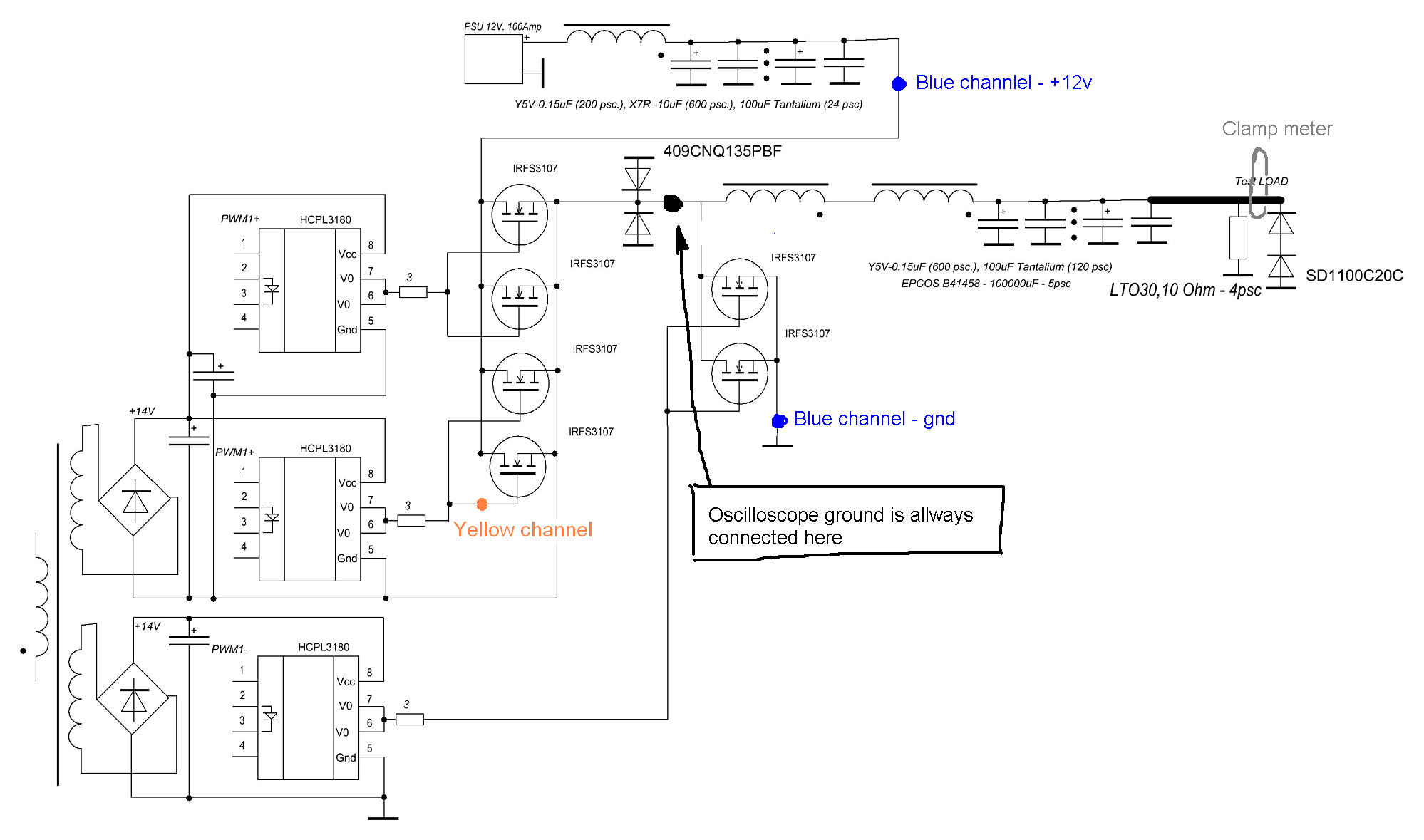
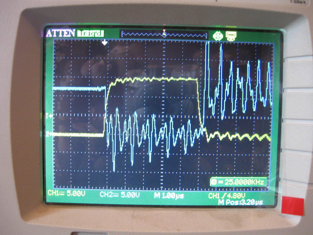
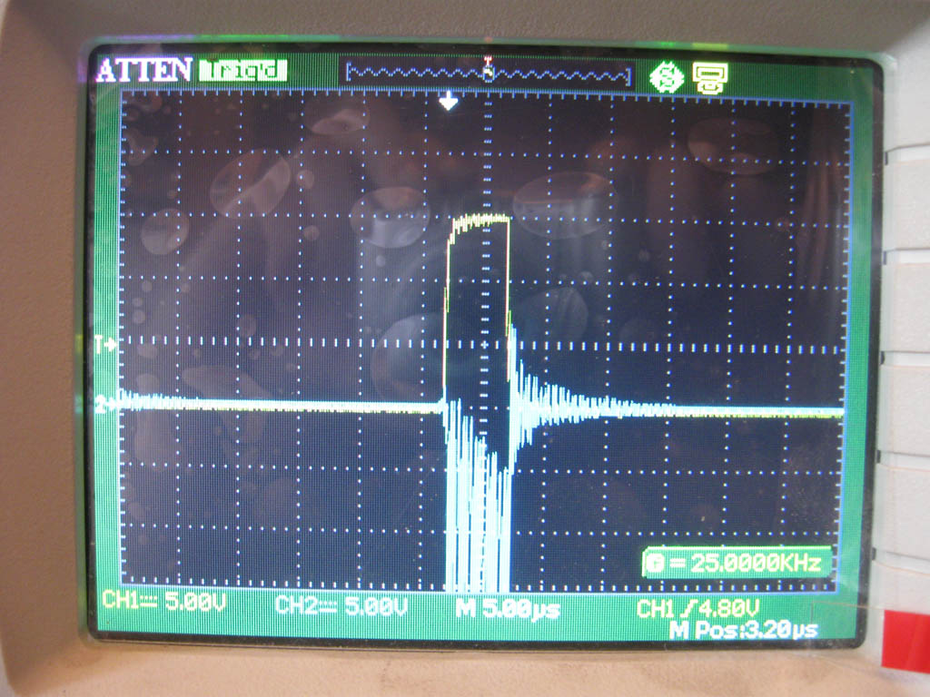
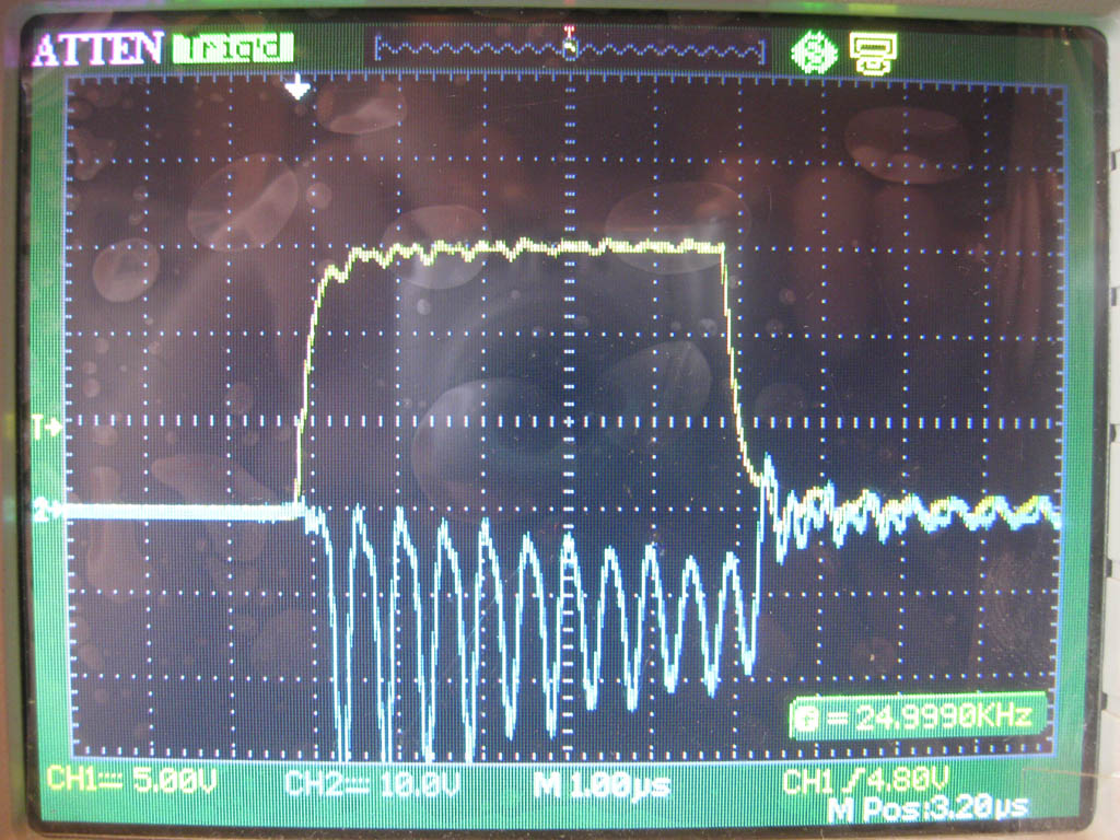
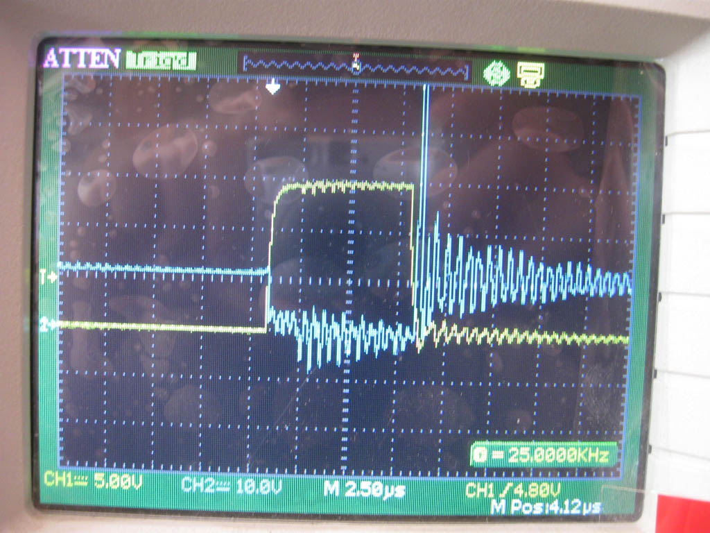
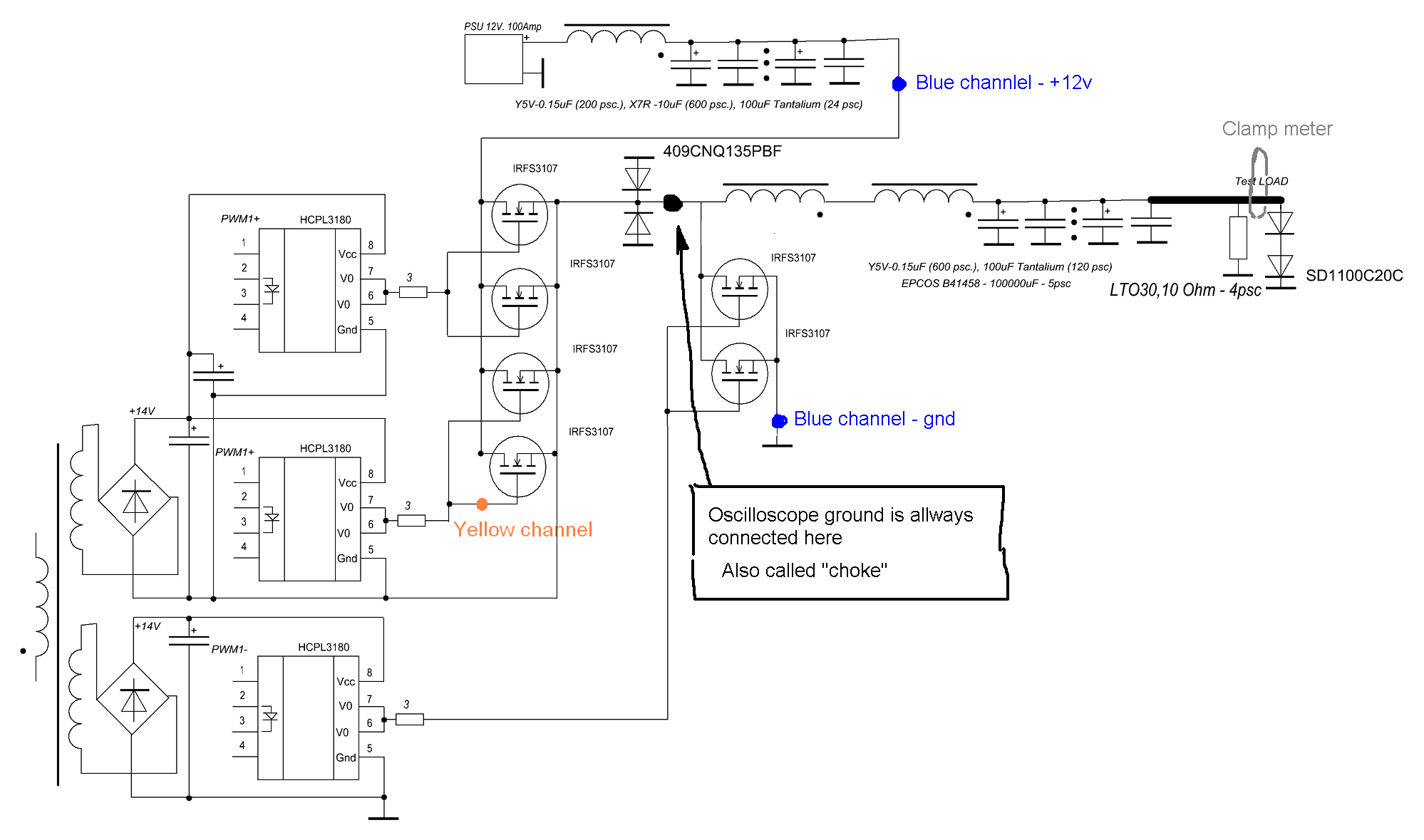
Hello. I build high power DC-DC PSU with digital PWM control. I want to get 150 Amps from 1 phase. Something does not work right – efficiency is 50%, mosfets heat much.
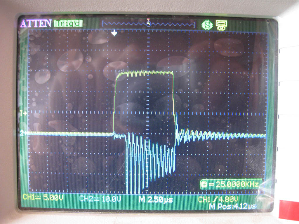
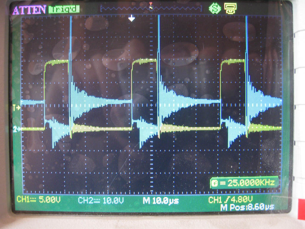
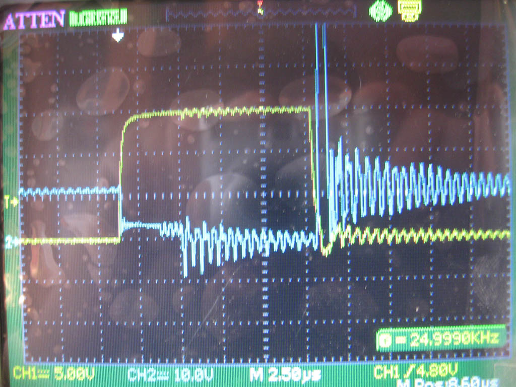
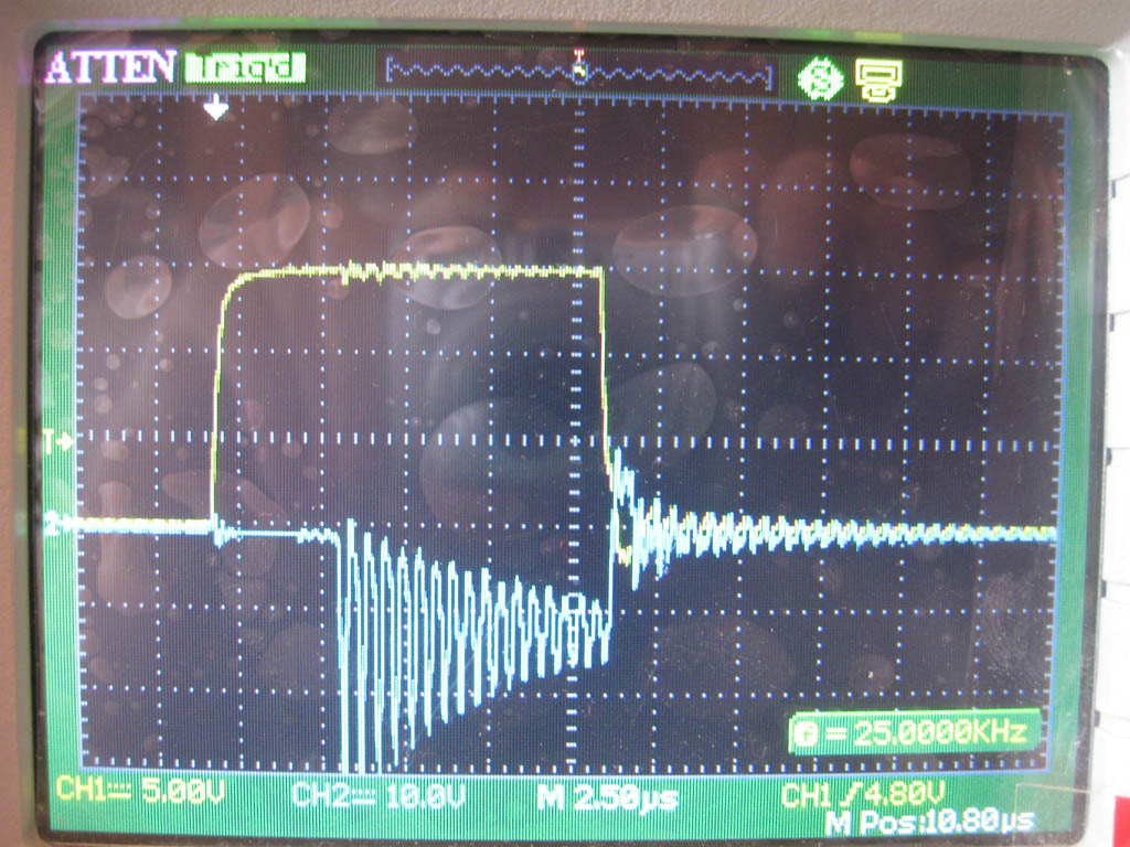
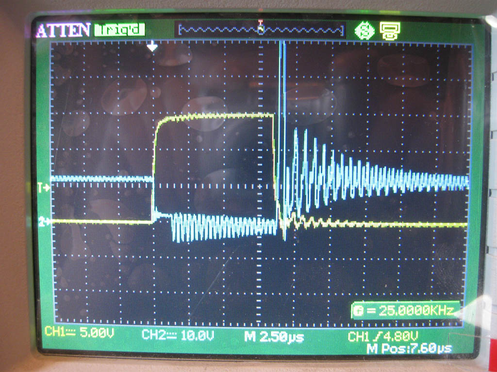
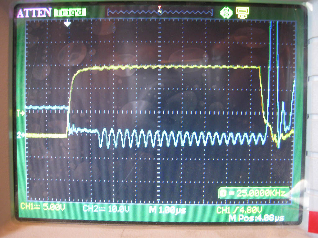
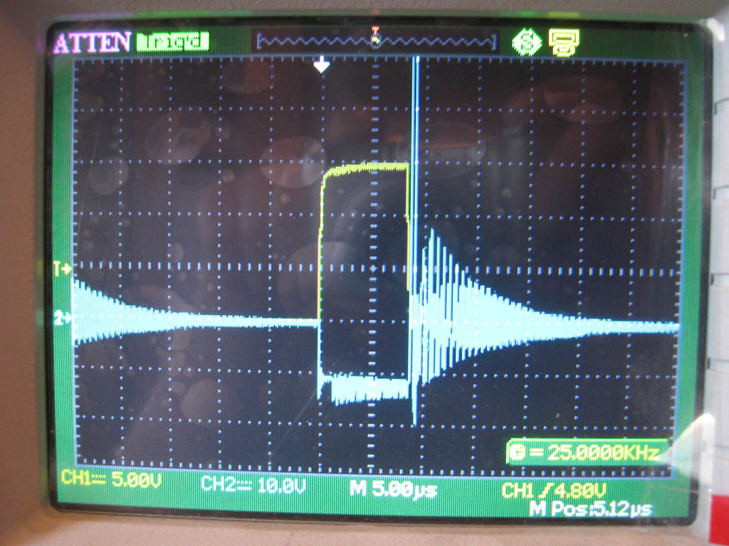
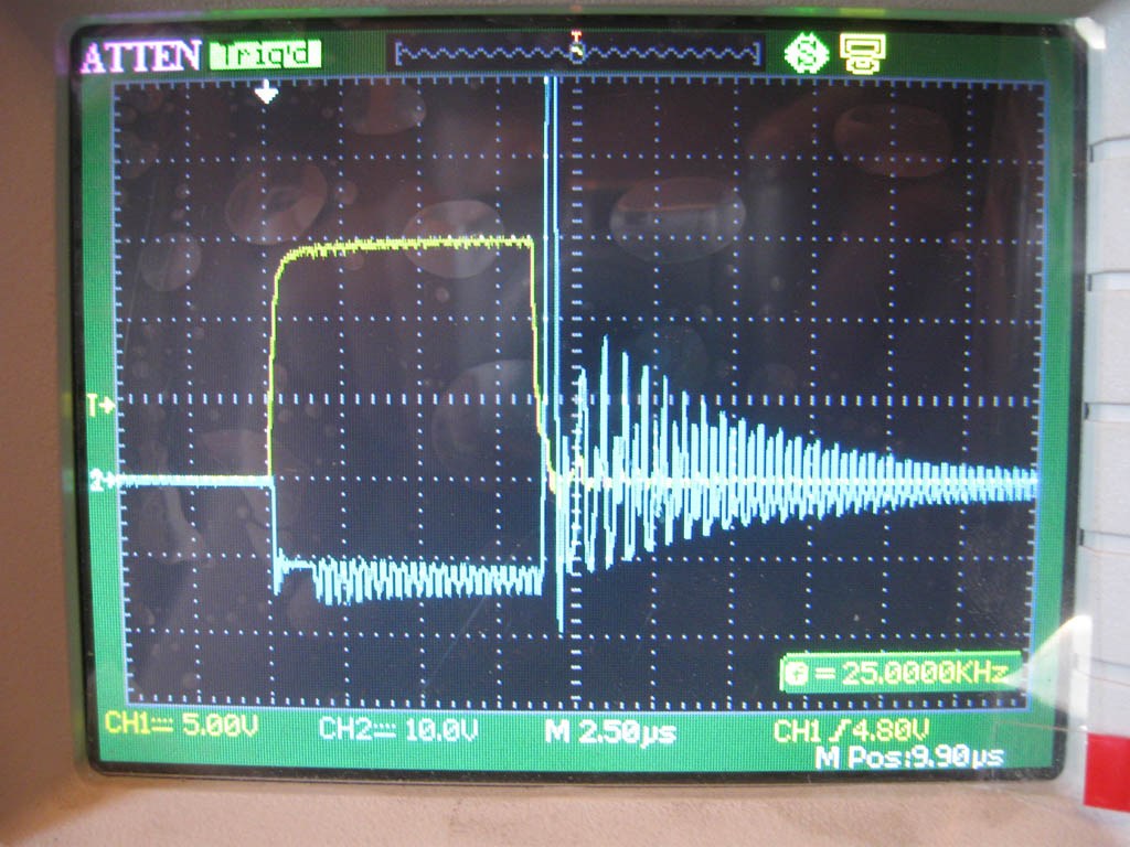
Frequency is 25khz; duty cycle on 1.76v 100amps load - 29.2%; 12v power supply current – 27.3 amps.
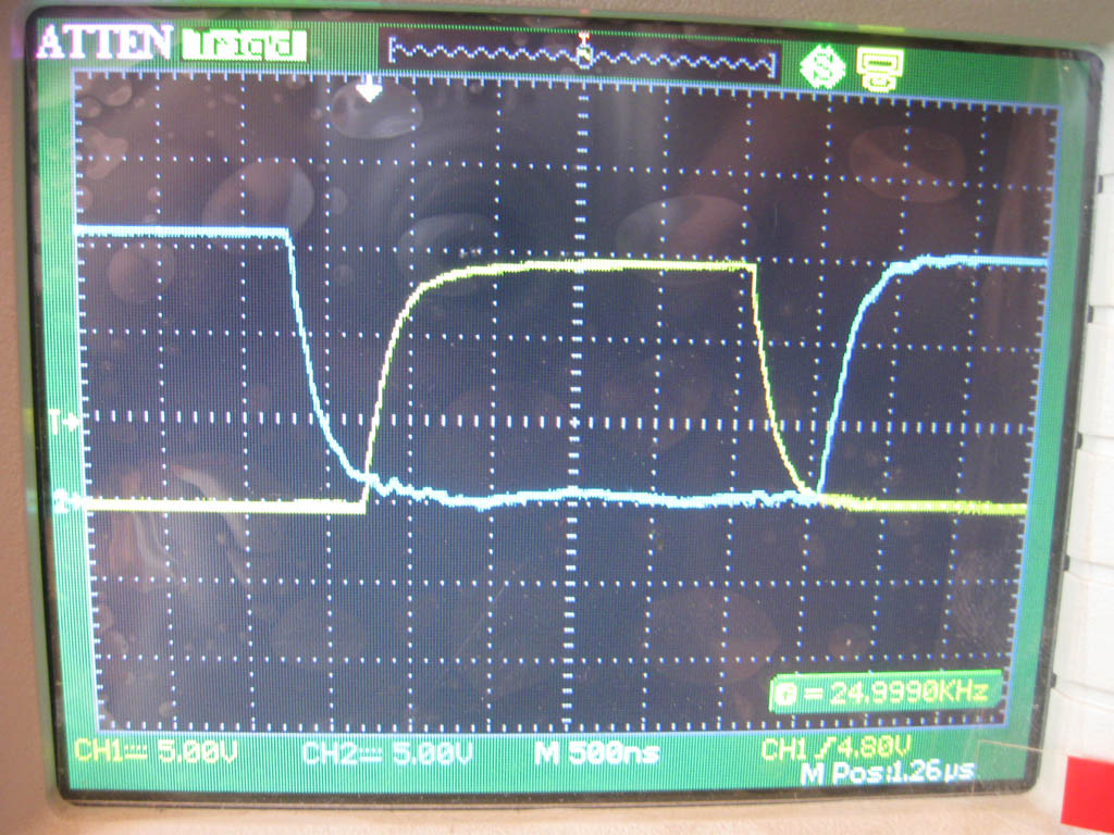
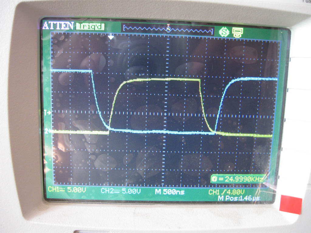
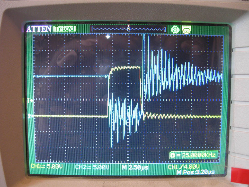
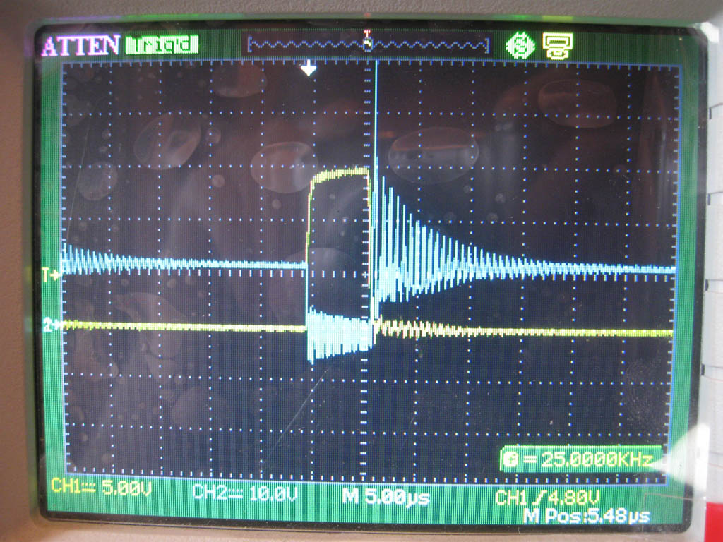
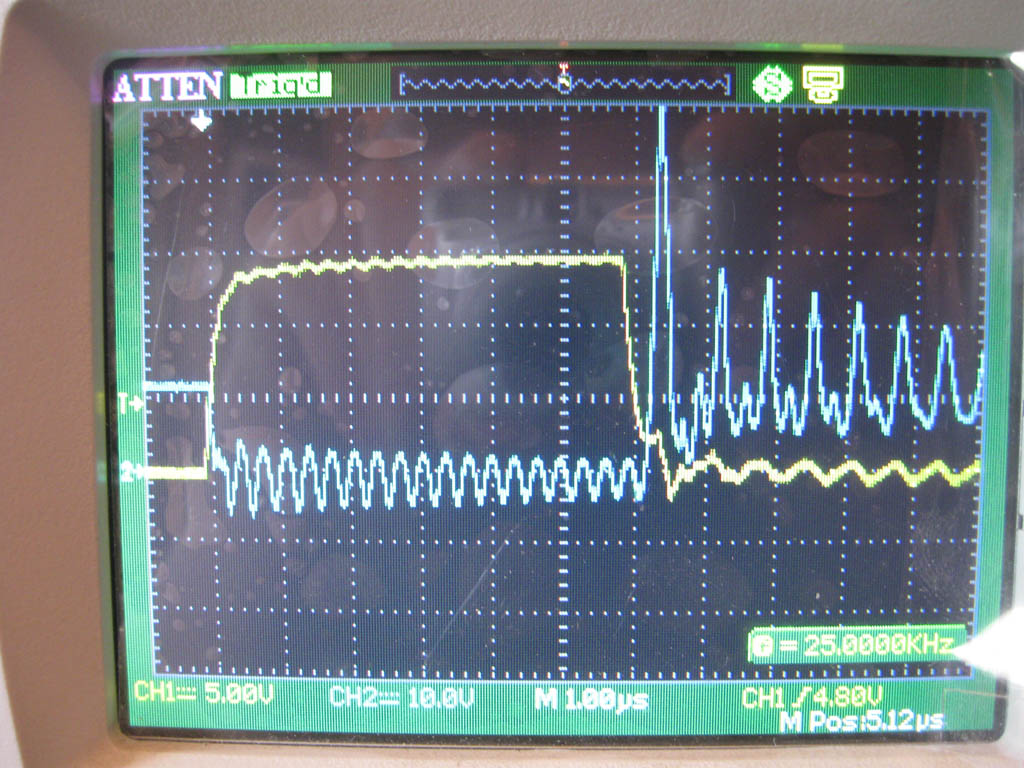
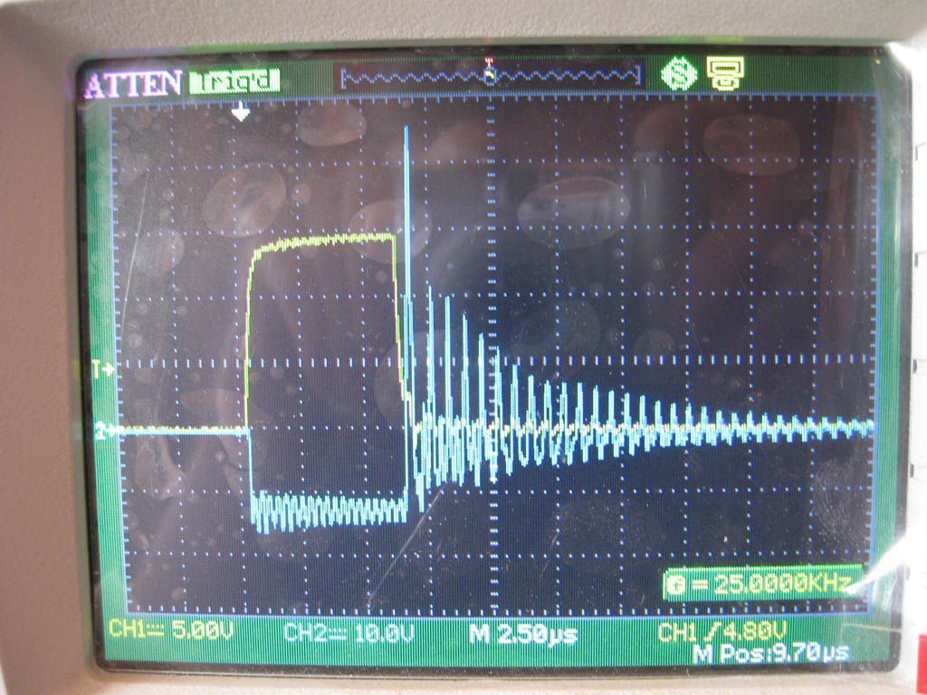
I post schematic with oscilloscope measure points. The second picture is gate-source voltage only. Reverse mosfets work well (100% no through current, they are cold with no cooling) but current divides in half between them and diode(DC current measured with clamp meter).
The choke has handmade frame for 4 E80 ferrites. There is 7.5 turns of double copper 0.5mm x 55mm tape. I don’t know real inductance of the choke – tests were with three series. Any results do not differ much with two chokes. Ferrites are on one side only. When tested tape was warm, ferrites – cold.
Please help me to understand what is wrong?!! 1.jpgforum_new.PNG2.jpg
 
Last edited:

Dear friend!
Hi
I think That your problem will solve with using snubber network in parallel with your mosfets(DS) because , the over shoot signal is very high. and its frequency is more higher than your PWM frequency. and i think you should create dead time in your PWM for optimizing your circuit. and it is better for you that use a resistance in parallel with GS of mosfets (for discharging GS capacitor) and when you wanna use parallel mosfets , you should use a very low resistance in series with Each source to decrease loss time (for matching the turn on time). and i don't know that what ia the value of your Series gate resistance ? if your resistance of gate (series) is high , your mosfets are not in saturation region as well as.
Best wishes
Goldsmith
 
Last edited:
I can't understand the waveform and testpoint relation. You say that yellow waveform is switched node and blue is gate voltage. But in the 2nd image (first waveform), the output seems to be turned on without gate voltage. Please clarify.
 

Dear Fvm - i fix mistake in the circuit label. Please, help: that type of the snubber network is necessary use in this circuit? In
**broken link removed**
i see many different variant. May be i must take RC parallel network? And one another question, about Series gate resistance. I use 3 om Resistor, without PullDown resistor, because output circuit of the hcpl3180 has low resistance with ground. It is correctly?
 
Last edited:

Exchanging the labels, the waveforms make more sense, and raise new questions. It looks like the high side transistor is switched on while the low side transistor is still activated (cross conduction). Reverse recovery time of the involved diodes should be much lower than observed 3.5 us.

Regarding snubber networks, they can help to reduce oscillations. You should be aware of the fact, that the oscillations are not the cause of low circuit efficiency. You can expect, that a snubber reduces the efficiency. In so far, you should first try to understand the real problems of your circuit. I fear, that besides possible cross-conduction, the circuit layout will be the main problem. The resonance frequency suggests rather large circuit inductances around 0.3 uH. Can you show a photo?

A starting point for an effective series RC snubber would be around 1-2 ohm / 50 to 100 nF, preferably splitted into multiple parallel RC circuits.

P.S.: The gate resistance order of magnitude seems basically reasonable. Faster gate drive would be possible but may also involve additional oscillations. Personally, I would always use individual gate resistors for each transistor.

As another comment the schottky diode cause 3/4 of the circuit capacitance and should be omitted favouring fully synchronous switching.
 
Last edited:

Dear friends
Again Hi
Snubber network will decrease the power dissipation( according to the press man book) . because in over shoot signals , mosfet wants to change the situation very fast and because its amplitude is high , mosfet wants to going to linear region. its dissipation will increase . if you damp them ( over shoots) your dissipation will be low. ( you should use non dissipative snubber (RCD) to correct it .
Respect

---------- Post added at 09:51 ---------- Previous post was at 09:43 ----------

If the series resistor with gate , become high , the voltage across the gs will going down , because of its capacitance .
and because of this effect , your mosfet will be at linear region.

---------- Post added at 09:52 ---------- Previous post was at 09:51 ----------

and linear region is so dissipative region
 

If the series resistor with gate , become high , the voltage across the gs will going down , because of its capacitance .
and because of this effect , your mosfet will be at linear region.
Do you mean to say, that 3 ohm is too high for the present application? What's your criterion for this statement?

Regarding "non-disspative" RCD snubbers, they are good to reduce overshoots. I doubt, that they will help much in the present situation.
 

Dear FVM
Hi
No my mean was not that 3 ohm is high! my mean is just that this resistance should become low . but 3 ohm is good .
Thank you
Goldsmith
 

Here are test of the psu.
I think something work very wrong there - please advice me a solution.

All tests output voltage is 1.6v(10amps) - 1.77v(100amps). Frequency is 25khz.

diode vs mosfet+diode
Code:
%duty  output(amps)  +12(amps)

3 chokes; half ferrites; reverse diode+mosfet

12.70   5   0.8
14.32  10   1.7
16.82  20   3.6
18.32  30   5.6
21.45  50  10.5
26.02  80  19.8
29.02 100  27.0


3 chokes; half ferrites; reverse diode only

15.01   5   1.1  
16.64   10  2.0  
19.07   20  4.3  
21.39   30  6.8  
25.52   50  12.8

2 chokes vs 3 chokes
Code:
%duty  output(amps)  +12(amps)

3 chokes; reserve mosfet+diode

18.26  30   5.8  
21.26  50  10.7  
24.14  70  16.5  
25.64  80  19.7  
27.08  90  23.0  
28.58 100  26.7  
30.08 110  30.7  
31.58 120  34.8  


2 chokes; reserve mosfet+diode

17.95   30   5.6  
20,76   50  10.4  
23,58   70  15.9  
24,89   80  19.2  
26,27   90  22.4  
27,58  100  25.9  
29,02  110  29.6  
30,33  120  33.4  
31,83  130  37.7

Schematic:


Gate voltage:

duty 6.07 gnd=choke --------- duty 6.07 gnd-choke shorted


Reverse mosfet + diode, 5amps:

+12-choke ----------------- +12-choke ------------------ gnd-choke ------------------- gnd-choke


Reverse mosfet + diode, 30amps:

gnd-choke ----------------- +12-choke


Reverse mosfet + diode, 100amps:

+12-choke ----------------- +12-choke ------------------ gnd-choke
 

I have difficulties to identify the probe connection for each waveform. It's also not clear to me, how you can connect the oscilloscope ground to a "hot" circuit node (switcher output) without affecting the measurement. Does it mean, the circuit is completely floating or do you use a differential probe?
 

Under each waveform there is info what to what point it is metered. All points are mentioned on schematic picture: "+12v", "choke", "gnd", "yellow channel". First word is probe connection point and second is ground connection point.
Unfortunatelly I have only atten ads1062cm oscilloscope. Yellow channel is synchronization with PWM impulse, driver has it's own power supply so gate voltage can be only measured with oscilloscope ground connected to source i.e. "choke" point.
What I can imagine is measure schematic drain-source voltage and choke-ground voltage. Of course I measure output dc voltage with multimeter. I would like to measure inner currents but I don't know how - I have shunt, 75mv -300amps - but EMI is much much higher, I see hundreds millivolts on oscilloscope on this shut not galvanically connected to the scheme.
About floating - oscilloscope is 100% galvanically disconnected from scheme and from power ground. So it does not matter what point I use as measurement ground. The picture is stable and for photos it was not stopped. If it's possible please advice another connecton of my oscilloscope.
I think the most necesarry for the scheme is snubber. But I still don't understand how to implement it. Please show me an example referring to my schematic.

I update the schematic (of course tests diodes were right connected, it's typo on picture):


Some info about construction: mosfets are solder mounted to copper bus, interconnection is dual or tripple 16mm^2 wires (AWG 5), capacitors are soldered in rows on long pcb with one 16mm^2 wire for two rows.

Here are waveforms with reverse diode only, mosfets are physically disconnected:

Reverse diode, 5amps:

+12-choke ----------------- +12-choke ------------------ gnd-choke

Reverse diode, 30amps:

+12-choke ----------------- +12-choke ------------------ gnd-choke ------------------- gnd-choke
 

O.K. the probe configuration seems clear so far. I understand, that the text "blue channel ground" has to be ignored.

I assume, that the floating oscilloscope ground point doesn't cause major waveform corruptions or even backlash to circuit operation, because the "choke" node is rather low impedance. But it's not the preferable way to probe a circuit.

So what do you see from the waveforms? The gate signal is basically O.K. Also the previously shown timing relation of high-side and low-side gate voltages looked good. But the switched node waveform, either displayed as +12V-choke or gnd-choke looks weird. That makes me refer to my previous comment about circuit inductances. You see, that the switched (choke) node is swinging > 50 V below ground, which can't happen, if the diodes are in effect.
 

Status
Not open for further replies.

Similar threads

Part and Inventory Search

Welcome to EDABoard.com

Sponsor

Back
Top