Continue to Site

Welcome to EDAboard.com

Welcome to our site! EDAboard.com is an international Electronics Discussion Forum focused on EDA software, circuits, schematics, books, theory, papers, asic, pld, 8051, DSP, Network, RF, Analog Design, PCB, Service Manuals... and a whole lot more! To participate you need to register. Registration is free. Click here to register now.

Fixing early setup violations

Status
Not open for further replies.

harel222

Newbie level 5
Joined
Sep 21, 2011
Messages
8
Helped
0
Reputation
0
Reaction score
0
Trophy points
1,281
Activity points
1,344
Hi all,
Im using SoC Encounter, and after placement + optimization i analyzed time and got about 1700 setup violations.
The thing is, that apart from 6, all the violations are input-to-register, and almost all of them includes a port named PHY_DATA[*].
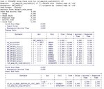
Example to a path from the report in the image.
TReport.JPG

And it continues with many path similar to this one.
It may be obvious (I'm a beginner), but what do you think i should do to solve it?
You can see in the second row in the table a delay of 4.888 ns which if i understand correctly is caused from PHY_DATA[5].. is this the problem?

Thanks a lot for your help.
 

Hi all,
Im using SoC Encounter, and after placement + optimization i analyzed time and got about 1700 setup violations.
The thing is, that apart from 6, all the violations are input-to-register, and almost all of them includes a port named PHY_DATA[*].
Example to a path from the report in the image.

View attachment 61721

And it continues with many path similar to this one.
It may be obvious (I'm a beginner), but what do you think i should do to solve it?
You can see in the second row in the table a delay of 4.888 ns which if i understand correctly is caused from PHY_DATA[5].. is this the problem?

Thanks a lot for your help.

Where is the clock period in the required time.
Check if the clock is defined properly or not?
 

The clock period is 10ns and u can see it in the report as Phase Shift (Upper left of the report).
 

Is it a memory block (RAM)? If so try bringing it close to the i/o port. this might fix a lot of violations for u.

It might even remove many buffers.
 

Thanks for the reply.
I don't have hard macros in my design. all the objects are stdcells that were auto placed by the tool.
Someone told me that the path connected to this port (PHY_DATA) might be too long so i should add buffers.. Does it sound right? and how do i place buffer manually i thought it is done automatically in the place/route..?
 

PHY_DATA* seems to be an input to your design, what transition rate are you using on inputs? Is there a long route from PHY_DATA[5] to the inverter that has the long delay time of 4.888ns?
 

Have you reported the same path in the synthesis tool?
Have you also reported the setup before placement to check you have the same setup marge as the synthesis tool seen?
After you could unerstand why so many buffer have been added not this path
 

Thank you both for your answers.
TonyLS, PHY_DATA is an input port. and if there is a long route from it to the inverter what can i do to solve it? about the inverter, should i replace it with a greater one in terms of fan out?
rca, all pathes in the the synthesis honored the timing constraints. what do u mean "reported the setup before placement"?
 

can u try moving the logic near to the input port?
 

in encounter, after library design preparation/loading you could made a timeDesign -prePlace, and you should see the same timing as the synthesis reported.
 

I cant move the logic near to the input port since it distributed all over the design.
rca, i did ran the command and got the same result as synthesis, no vios.
 

I am seeing that the first inverter in the path is taking almost 5ns delay. that is too much delay.
I am also seeing that ur design has zero slew at the input right?
Then i guess the load driven by the first inverter is huge.
Try seeing the fanout of the first inverter and if possible try cloning that inverter.
 
I am new to this tool and I also have the same doubt. Placing and routing is done by the tool automatically. How can we insert buffer in the design or bring some cells close to the input port?
 

During the optdesign phase, the encounter will add/increase drive of the cell to meet the timing.
 

Status
Not open for further replies.

Part and Inventory Search

Welcome to EDABoard.com

Sponsor

Back
Top