mr_l
Newbie level 5
Hello I am new to this forum although I have used this site for some time.
I got stuck with the following task and need some help.
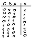
I have to draw a transistor diagram of a CMOS gate with the following logical
function
F (a, b, c) = (a * b + a * c + b * c) '
The gate must be made up of only One pull-up and a pull-down network. It should be connected in the same step not be linked to several steps with AND, OR and NOT gates in succession, one after another.
I am not asking anyone to solve my task
I have read and been understanding how CMOS transistors working
but I was a little difficulty to construct the gate. Is it any particular method for constructing logic gates???
