Continue to Site

Welcome to EDAboard.com

Welcome to our site! EDAboard.com is an international Electronics Discussion Forum focused on EDA software, circuits, schematics, books, theory, papers, asic, pld, 8051, DSP, Network, RF, Analog Design, PCB, Service Manuals... and a whole lot more! To participate you need to register. Registration is free. Click here to register now.

Potentiometer Footprint issue on PCB Editor

Status
Not open for further replies.

tiwari.sachin

Full Member level 6
Joined
Aug 1, 2009
Messages
341
Helped
3
Reputation
6
Reaction score
3
Trophy points
1,298
Location
India
Activity points
4,449
Hello

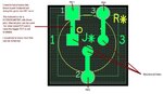
I am using orcad 15.5 and i am trying to design the footprint for the potentiometer.

This has 3 pins. I decided to have 3 extra holes and interconnect them so that the internal pins can be used for small sized potentiometer when the bigger size pot is not available. Attached is the footprint for reference.

Can somone let me know if i can have tracks/line on etch layer while creating the footprint itself and how can i made sure that pins are interconnected without getting the DRC
 

Attachments

  • Potentiometer Footprint.JPG
    Potentiometer Footprint.JPG
    70.4 KB · Views: 202

I don't use Orcad but a similar problem exists in Eagle. You want to create a footprint but that creates errors. In Eagle you just accept it and can "approve" the errors and the warning won't appear again. However, there is another option.

Create a part with 6 pins. Just put the pads for the pins in the footprint. Put the tracks in the layout. I think that should give you an error free layout (but a messier looking schematic as you now how a 6 pin pot).

Keith.
 

I would use two pots then make one a non fitted, advantage is when you are creating a BOM you can specify implicity which is fitted and which isn't. I have variant manager in Cadstar that makes this easy, cant remember how we did it in Cadence, but we did somthing similar.
 

Keith,

Having a pot with 6 pins.. well i thought of it but very messy looking. We are more used to seeing POT with three pins. 6 pins doesnt seem to be better option.


Marce,

You would want to use two POT and show that in schematic as not connected to any parts at all... Placing one part over another while routing... I dont think i am looking for this option. Doesnt sound feasible....
 

Doesn't Cadence has an option to assign multiple physical pins to a symbol terminal as other full featured PCB design tools have?
 

No, have two pots on the circuit, you then have two variants of the design, one variant would have one pot fitted the other not and visa versa. This is the best way to manage situations like this on designs so that you can controll them properly. You could also put a not on the schematic explaining the reason for two pots. I haven't used Cadence tools for over 2.5 years now so I'm a bit rusty on the process, but the following link may help, or searches for +Cadence +"variant manager"
EDACafe.com: Videos - EMA Design Automation : Design Variant Management using Cadence OrCAD Capture CIS - EMA Design Automation

Or where I total control of the BOM is not required from the schematic, use the dual footprint method, for prototyping and development it perfectly acceptable.
 

Hi sachin,
I also faced problem same as like you.... I am working with cadence16.3....
I am also having doubt that can I put track/line in foot print itself??.....
Please answer this and then we can go for solution..
 

Many years ago I did a similar thing with capacitors where I needed the flexibility to change the physical size (due to the large range of values to be accommodated).

55_1315987207.gif


Keith.
 

Many years ago I did a similar thing with capacitors.
How does it appear in the schematic symbol? I would expect 4 pin numbers (if display is activated) for one capacitor terminal.

It's similar with the below shown part, that represents a through hole or SMD capacitor as assembly variants. Pin numbers are normally hidden. Pin wiring is done as regular board routing in this case. In fact I don't want to decide in the foot print editor which layer has to be used to connect the pins.

85_1315988088.gif


P.S.: The routed component looks like this

76_1315988635.gif
 
Last edited:

Yes, it has 5 pins in total. I think you can overlay the pins but some packages (e.g. Eagle) won't let you put a pin on top of a pin in the schematic view.

Keith.
 

Hi,
keith and FvM, please let me know....can I put track/line in foot print itself....??
When I am doing artwork, its diaplaying DRC there.... Please help me.....
 

can I put track/line in foot print itself
In most tools, you can't. I don't think that it's generally useful however. You have many parts with multiple pins for one logical terminal, they are usually routed regularly. This gives the option to decide which layer to use. In special cases, copper pour in the footprint may be an option.
 

You can put tracks in Eagle footprints but you get DRC errors. You can "approve" the errors so you aren't shown them from then on. The only time I tend to do that is when creating weird shapes such as the pads of some surface mount inductors.

Keith.
 

you mean copper pour shape there instead of track??
 

Yes marce, its working . thank you so much for help.
 

I am sorry for not being able to reply till now. I have managed to create the gerbers with the DRC errors and it worked all fine but at the end of the day having two pots and two separate footprints and overlapping them seems to be a better option.
 

Status
Not open for further replies.

Part and Inventory Search

Welcome to EDABoard.com

Sponsor

Back
Top