Continue to Site

Welcome to EDAboard.com

Welcome to our site! EDAboard.com is an international Electronics Discussion Forum focused on EDA software, circuits, schematics, books, theory, papers, asic, pld, 8051, DSP, Network, RF, Analog Design, PCB, Service Manuals... and a whole lot more! To participate you need to register. Registration is free. Click here to register now.

High side P-MOSFET power switch

Status
Not open for further replies.

leekc_84

Junior Member level 3
Joined
Sep 18, 2006
Messages
25
Helped
1
Reputation
2
Reaction score
1
Trophy points
1,283
Activity points
1,430
Hi,

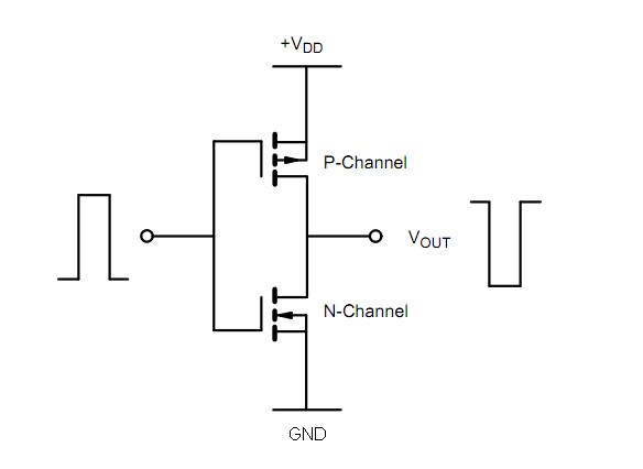
I am thinking to do a very simple high side p-mosfet power switch. Let say Vcc 5V to source, gate voltage controlled by FPGA output, and the load current is about 0.5A at the the drain, parallel with filtering capacitor.

What specific precautions will need to take care? How to determine MOSFET parameters in order to get fast turn on/off time?

Thanks for help.
 

you need to specify the gate thresholg voltage Vgs(th)in order to apply to the gate to turn ON the MOSFET, and you have to specify the current Ids, to get a fast turn on/OFF you have to ensure a current that will be enable to charge fastly the parasitic capacitor ( miller effect), and choose a transistor with w low gate charge ( explained in C)

---------- Post added at 16:15 ---------- Previous post was at 16:11 ----------

also take a look at this, i think this will clear your doubt
https://www.fairchildsemi.com/an/AN/AN-9010.pdf
https://www.fairchildsemi.com/an/AN/AN-9068.pdf
**broken link removed**

---------- Post added at 16:15 ---------- Previous post was at 16:15 ----------

also take a look at this, i think this will clear your doubt
https://www.fairchildsemi.com/an/AN/AN-9010.pdf
https://www.fairchildsemi.com/an/AN/AN-9068.pdf
**broken link removed**
 

Thanks Yassin. Do you think FPGA driving capability will matter?
 

it depends in the voltage that the FPGA can output, you should ensure that the voltage that the FPGA output is more then Vgs ( th), and also it depends on your MOSFET, you should insert a MOSFET driver
 

Thanks Yassin. Do you think FPGA driving capability will matter?

You haven't specified the intended use for the mosfet, if you are going to use any king of fast rate switching then you will need a driver but if you just want to use the mosfet at a slow rate like a few dozen times per second or slower then you can probably drive it directly from the fpga.

Note that there is also the alternative solution of a smart high side switch ( High Side Switches - STMicroelectronics ), the benefits are lower Rds-on because they use N-mosfet, no driver since they are implemented internally and also can be driven from logic level voltages, the price will be higher than a simple mosfet obviously.

Alex
 

Thanks Yassin & Alex.

The mosfet is just for a simple load switch, not for fast rate switching e.g. PWM. Thus FPGA would be good enough.

By the way, I am not sure how to determine turn on/off time for the load if just based on MOSFET datasheet. Does it related to the switching characteristics stated in datasheet?
 

The MOSFET datasheets have a factor called Total Gate Charge and is given in nC.
It is actually the time * current at which the MOSFET is fully on, for example when you read 100nC it means that if you give 1A (limit the gate current to 1A is what i mean) the gate will be charged after 100ns (100nC /1A = 100ns ) or if you give 10mA the gate will be charged after 10000ns (100nC /0.01A = 10000ns ) etc

also check
https://www.fairchildsemi.com/an/AN/AN-9010.pdf
see page 17 for the different gate capacitance charge stages

Alex
 

Thanks Alex.

-deleted-
 
Last edited:

Hi all,

I have a question. After turn off the switch, the load voltage should be close to zero volt. But somehow there's leakage from other voltage source, the load voltage stays at 2V. (Imagine on-off the switch, load voltage swing from 5V to 2V, and 2V to 5V... never reach to zero.

Is there any recommendation to solve this issue (not going to amend load condition)?

I am thinking totem pole would help to solve (as in pic)?


Please suggest, thanks in advanced.


Tried this circuit, and it works fine!
 

Somehow I found that this circuitry not so stable... when designing complementary MOSFET switch, what parameters are important?

Here are some I suspected:
- Vgs for both FETs need larger to avoid switch on at the same time
- Rds for PMOS has to small in order to avoid voltage drop

Anything I missed out? For NMOS what should need to pay attention?

-Add on-
Found out that the gate voltage will drop about 0.5V when driving two MOSFETs simultaneously. How could this happen?
 
Last edited:

Status
Not open for further replies.

Similar threads

Part and Inventory Search

Welcome to EDABoard.com

Sponsor

Back
Top