Continue to Site

Welcome to EDAboard.com

Welcome to our site! EDAboard.com is an international Electronics Discussion Forum focused on EDA software, circuits, schematics, books, theory, papers, asic, pld, 8051, DSP, Network, RF, Analog Design, PCB, Service Manuals... and a whole lot more! To participate you need to register. Registration is free. Click here to register now.

sar adc capacitor leakage current

Status
Not open for further replies.

pianomania

Member level 5
Joined
Jun 15, 2006
Messages
83
Helped
0
Reputation
0
Reaction score
0
Trophy points
1,286
Activity points
1,906
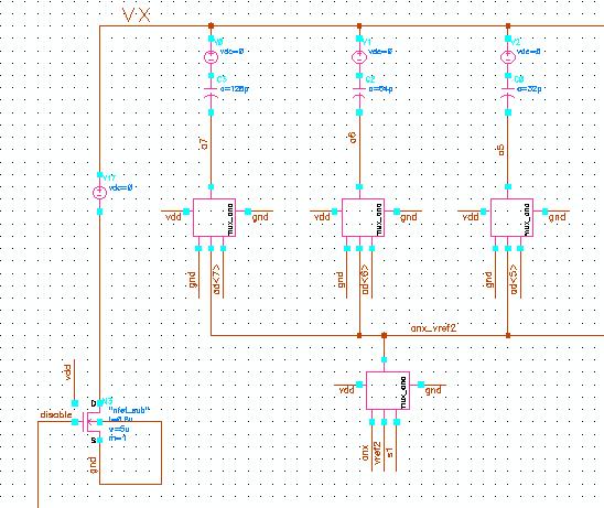
i design a cap type charge sharing sar adc ,
it needs to be dischage when each conversion cycle.
please see the pic show as below ,
the node vx=0 when sampling mode , and it is pull down by N3.
but when the hode mode , the N3 should be disable.

but , since the vx will be negative voltage , the MOS N3 body diode will flow to have a leakage..

how to solve this problem , to replace the switch in another kind of solution ?


... since the vx will be negative voltage , the MOS N3 body diode will flow to have a leakage..

how to solve this problem , to replace the switch in another kind of solution ?

Connect N3's bulk to the drain instead of to the source.
 

thank you for your advice,
but the vx is not always negative voltage, sometime the voltage is greater than zero , sometimes less than zero , when normal operation.
thus ,the soultion may not work
is there any other solution for this ?
 

... the vx is not always negative voltage, sometime the voltage is greater than zero , sometimes less than zero , when normal operation.
thus ,the soultion may not work

Anyway, such a connection requires a twin (double) or triple well process which allows for isolated NMOSFETs. If the process also provides Schottky diodes, you could connect 2 Schottky diodes from source and drain to bias the bulk to the most negative potential (both anodes to bulk).

In this case it doesn't matter if vx is positive or negative against GND : No current can flow then between vx and gnd (when N3 disabled). The Schottky diodes will always bias the bulk appropriately, but this also means the terminal which biases the bulk is the real source, and, thus, the reference terminal for the control signal ("disable").

is there any other solution for this ?

If the process doesn't allow for isolated NMOSFETs -- but provides Schottky diodes -- you could use a PMOSFET as switch, bias its bulk (n-well) by 2 Schottky diodes (both cathodes to n-well) and invert your control signal. Be aware you have to refer it to the most positive potential, either vx or gnd .

BTW: If gnd-0.5V ≦ vx ≦ gnd+0.5V you need not change anything! ;-)
 

thank for your help.
but i found another current conduction path , not relative to the body diode.
since the gate voltage of the charge MOS (disable) has two voltage , 0 and vdd , the 0 is for disable the dischage MOS. but in this situation, the MOS is not disable , since the drain is negative voltage , gate voltage > drain , the mos can be "reversed conductive". not through the body diode..
thus by switch the bias of the buck can't solve the unwanted leakage.
if we change it as PMOS , the phenomenon still exists.

and if we add diode serial connect with , when the dischage phase , the VX can't be pull down and discharge to Zero.

so , could you find another method to solve this problem?
 

... since the gate voltage of the charge MOS (disable) has two voltage , 0 and vdd , the 0 is for disable the dischage MOS. but in this situation, the MOS is not disable , since the drain is negative voltage , gate voltage > drain , the mos can be "reversed conductive". not through the body diode..
Right, but only if |vx| > Vth .

if we change it as PMOS , the phenomenon still exists.
Correct.

and if we add diode serial connect with , when the dischage phase , the VX can't be pull down and discharge to Zero.
Of course not.

so , could you find another method to solve this problem?
If |vx| > Vth it seems you must have available somewhere a negative voltage? If so, you could use it to disable the NMOS.
Otherwise: use a different topology!
 

Status
Not open for further replies.

Similar threads

Part and Inventory Search

Welcome to EDABoard.com

Sponsor

Back
Top