Continue to Site

Welcome to EDAboard.com

Welcome to our site! EDAboard.com is an international Electronics Discussion Forum focused on EDA software, circuits, schematics, books, theory, papers, asic, pld, 8051, DSP, Network, RF, Analog Design, PCB, Service Manuals... and a whole lot more! To participate you need to register. Registration is free. Click here to register now.

Gerber file check before manufacturing

Status
Not open for further replies.

blitzsk

Newbie level 3
Joined
Dec 2, 2010
Messages
4
Helped
0
Reputation
0
Reaction score
0
Trophy points
1,281
Activity points
1,314
I Have used EAGLE CADSOFT to layout this board and I think I'm almost done with it , But I'm not sure if my design rules are proper or not. so i have attached my *.brd and also drc rules. I have used multiple polygons for power planes in the same plane , so its not a standard power plane ($gnd,$vcc..etc) . this is my first board and the cost of manufacturing it is high so i dont wanna make any mistakes.. Any suggestions, comments are welcome.
I have attached the *.brd file , drc , and gerber files.
 

Attachments

  • New folder.zip
    458.3 KB · Views: 89

Two comments.
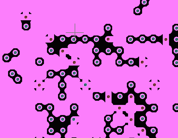
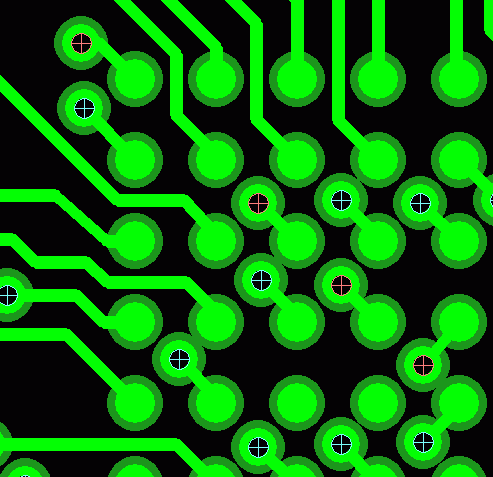
- You have solder mask openings for vias. They may be required by your PCB manufacturer, but you should reduce them to a size slightly larger then the drills to achieve sufficient pad to via spacing, particularly under the BGA. Alternatively the solder mask enlargement has to be reduced. Otherwise there's a high risk of BGA balls being sucked into via holes.

88_1313441478.gif


- It's recommended to remove unconnected via and pth pads on inner layers. But if dynamic pad and vias are not supported by your tool, it can be done by the PCB manufacturer.

0_1313441499.gif


In adition, it seems to me, that the blind via option won't be strictly required for this design, because there's plenty of room for standard vias.

P.S.: As a minor point, you would want to have a separate outline plot with your gerber file. But it can be extracted from the silk screen plots.
 
Last edited:
I have had a look at the Eagle files and there are not problems I can see - you have obviously got the design rules from Sunstone so that saves making any mistakes creating your own. By the way, when you load the design rules into your PCB they stay there so you don't need to include the .dru file any more.

Some of the routing looks untidy but it is only aesthetic - non 45 degree tracks and tracks going round vias that aren't there any more.

A frame around the schematic usually looks better and allows you to keep it to a certain size such as A3 and add title, date copyright and revision data. If it gets too big you can split it into multiple pages. That is probably for later but if you want to split into multiple pages with an existing circuit/layout, let me know and I will explain the method you must use to preserve the link between the schematic and layout.

I must admit I would have kept more than 5mil spacing between the polygons, but it should manufacture ok. Hot air levelling used to make shorts from power planes more likely in my experience but I would guess you will be using ultra flat tinning.

I agree with FvM abut the blind vias. I Changed them all to normal and it produced 24 errors but they were all easily fixed. You could save a lot of money making the PCB by using a conventional 6 layer.

If you want solder resist over your vias then increase the "limit" value on the MASKS tab of the DRC. Any drill smaller than LIMIT will have solder resist.

Keith.
 
Thanks a lot Fvm and keith ... its my first board and I had 45 degree's everywhere but I kept moving things around to shrink the board and I dont mind the looks of the board as long as it works... and I agree the board can be done without blind vias I tried initially but there were few deadlocks and I either had to reassign all the pins or go with blind vias , i went with the later . Anyways i found a board house that is doing my board for 60$ so the cost isnt a problem.

I have another question , how am I supposed to see the holes(*.drl gerber files) in 1:1 ratio so that it matches with the vias and drills of the other layers ? . I tried using pcb investigator and teamviewer for the gerber files , is there anything that you recommend ?

---------- Post added at 22:10 ---------- Previous post was at 22:04 ----------

How do I Increase the isolation between the polygons ???
 

I have another question , how am I supposed to see the holes(*.drl gerber files) in 1:1 ratio so that it matches with the vias and drills of the other layers ? . I tried using pcb investigator and teamviewer for the gerber files , is there anything that you recommend ?

I use the free version of GC-prevue GraphiCode - Software Innovations for Electronics Manufacturing - Home

You need to make sure you load the drill files as well as the Gerber files. Also, sometime the software will misinterpret the data and you need to manually over ride the settings. On a drill, for example, it may think values are 2 digits plus 4 digits after the decimal point when in fact they are 1+5. Also, make sure you avoid some of the spurious "report" files - the gerber viewer should throw up an error with them but it saves time if you know which ones to load.

[/COLOR]How do I Increase the isolation between the polygons ???

Increase the ISOLATE value for the polygon. At the moment it is zero which means it will use the minimum allowed under the design rules.

Keith.
 
  • Like
Reactions: FvM

    FvM

    Points: 2
    Helpful Answer Positive Rating
The above displayed gerbers plots in post #2 are GCPrevue screenshots. The tool sizes have been read-in from your Eagle gerber files automatically.
 

They loaded fine for me into GCprevue as well. I don't often have problems with Eagle's Gerbers - just the occasional misinterpretation of the drill digits which is easily fixed when it happens.

Keith
 

Status
Not open for further replies.

Part and Inventory Search

Welcome to EDABoard.com

Sponsor

Back
Top