Continue to Site
Follow along with the video below to see how to install our site as a web app on your home screen.
Note: This feature may not be available in some browsers.
You can't really check this for timing-it's indeterminate (even if you know all the propagation delays, etc) because of the non-integer relationship between the two clocks. Is this an FPGA or ASIC design? If so, then depending on the specifics of this circuit you may want to give it a relaxed constraint (like a multi-cycle or ignore). However, if this is a critical path then you're going to have to add a synchronizer or FIFO. There's no way (that I'm aware of) that you can guaranteed the exact timing of the output of the second ff. Using your timing diagram above, after the first A clock edge data will appear at the D input of the B ff. But at time 6, NEW data will be clocked out to the D input of B. Thus, the output of the B FF after the B rising edge at time 8 will be the SECOND data bit from A; the first one never gets clocked into B. Classic multiple-clock-domain problem.
I suggest you either add a FIFO or a multi-cycle constraint. You've got two different data rates. If the input rate were the slower one then it would be a different story (but still messy). There's a lot of info out there about clock-domain crossing, synchronizers, etc. Check them out.
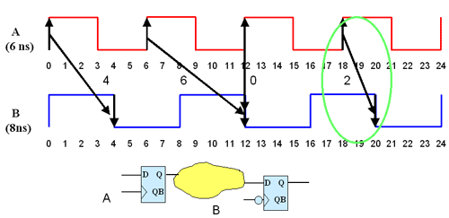
You cannot do a timing analysis on async paths. That's the nature of asynchronous logic and data gets captured by whatever clock edge available.I think we can still check timing for these two flops. I don't agree with Barry. One thing most people here are confusing is that both the FFs are not positive edge triggered. Launch flop is rise edge triggered and capture flop is Falling edge triggered. Also, the two clocks are in phase, c'mon see the edges lining up at 0 and then 12ns and again at 24ns. Let's not get all delusional instead lets stick to the given facts. The reason that the figure has waveform drawn for 24ns is because the LCM of 6 and 8 is 24. Next, you gotta figure out what the cycle adjust is between the two clocks. Its ofcourse not a full clock cycle, neither is it half of 6 ns or 8ns clock. Cycle adjust calculation is what is shown how it is calculated. Possible candidates are:
1. Data launched at 0ns and captured at 4ns. This gives 4ns as candidate.
2. Data launched at 6ns and captured at 12ns. This gives 6ns as candidate but since we already have lesser value from #1, throw it out.
3. Data launched at 12ns and captured at 12ns. This gives 0ns as candidate but its not accepted as cycle adjust, throw this out too.
4. Data launched at 18ns and captured at 20ns. This is less than #1 and hence the correct cycle adjust.
What cycle adjust of 2ns will mean is that, there can only be data path delay of 2ns on this path (assuming zero clock skew) to avoid setup violation.
Hold timing doesnot depend on clock frequency so lets leave that out.
If its greater than 2ns, manipulate clock skews.
Thanks,
You cannot do a timing analysis on async paths. That's the nature of asynchronous logic and data gets captured by whatever clock edge available.
So, analyzing the timing in the above diagram with 2ns cycle window has no value.
Furthermore, if the logic meets 2ns path delay as you said, you would have a hold violation at 6ns to 8ns.
Why you call the clocks asynchronous, What more do you you ask for when the waveform edges line up as they are shown.
I never said there would be a hold violation. Its not dependent on your clock waveform - all that is there. A 2ns data path delay normally should not normally have hold problem.