haircream
Newbie level 1
Hi guys,
I am doing a subject assignment in Uni.
I need to design a barrel shifter (4X4). I done the circuit and now i try to draw the layout and met some weird problem.
BTW: i am using IC station on RedHat.
For your information, while drawing the layout you can invoke the logic (circuit) and put it beside the layout you gonna draw to have a better view. If you click on any of the wires, the blocks (components like MOS) that connected by it will be highlighted and there is a yellow line that connecting them as a guide.
Now that I need to ground the NMOS i use to build the shifter I found out that none of the block is highlighted (the instance of a NMOS - 1 red poly in the mid and 2 metal 1 at the site) but there is a yellow connecting the MOS - from poly to poly but nothing is being highlighted.
So how should i ground it ? As almost all the poly are connected to something else, ie: input or output. How could any wires be shorted straight to ground ? this dosnt make sense and therefore i cant pass the LVS.
I hope you guys understand what I am trying to say and please help me > <.
Attachments:
1. **broken link removed**
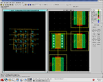
This is an example when a line is click and all the those blocks that connected by it will be highlighted. Note that for this case one of the control input is being click and the relevant
poly (red one) is being hightlighted as well as the yellow guide line.
2. **broken link removed**
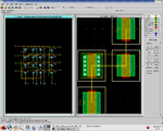
This is the problem i am facing - i click the gound and just the yellow guide line being highlighted (i dont even sure is that a guide line) and the dotted line that enclosing the NMOS is highlighted as well which i dont understand what does it mean.
3. **broken link removed**
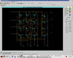
This is the circuit of the barrel shifter i am working on. Note that is all NMOS no PMOS is used - would it be a problem ? cause i think we just need to ground the NMOS instead of putting PMOS cause need to supply VDD. That's how i come to this.
Thanks.
I am doing a subject assignment in Uni.
I need to design a barrel shifter (4X4). I done the circuit and now i try to draw the layout and met some weird problem.
BTW: i am using IC station on RedHat.
For your information, while drawing the layout you can invoke the logic (circuit) and put it beside the layout you gonna draw to have a better view. If you click on any of the wires, the blocks (components like MOS) that connected by it will be highlighted and there is a yellow line that connecting them as a guide.
Now that I need to ground the NMOS i use to build the shifter I found out that none of the block is highlighted (the instance of a NMOS - 1 red poly in the mid and 2 metal 1 at the site) but there is a yellow connecting the MOS - from poly to poly but nothing is being highlighted.
So how should i ground it ? As almost all the poly are connected to something else, ie: input or output. How could any wires be shorted straight to ground ? this dosnt make sense and therefore i cant pass the LVS.
I hope you guys understand what I am trying to say and please help me > <.
Attachments:
1.
 **broken link removed**
This is an example when a line is click and all the those blocks that connected by it will be highlighted. Note that for this case one of the control input is being click and the relevant
poly (red one) is being hightlighted as well as the yellow guide line.
2.
 **broken link removed**
This is the problem i am facing - i click the gound and just the yellow guide line being highlighted (i dont even sure is that a guide line) and the dotted line that enclosing the NMOS is highlighted as well which i dont understand what does it mean.
3.
 **broken link removed**
This is the circuit of the barrel shifter i am working on. Note that is all NMOS no PMOS is used - would it be a problem ? cause i think we just need to ground the NMOS instead of putting PMOS cause need to supply VDD. That's how i come to this.
Thanks.
Last edited: