legend4566
Newbie
Hi everyone, this is my first post.
I have a some problem encountered during my homework. I have no idea where to post it so if its not in the appropriate sub-forum please help me move it mods =)
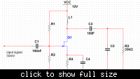
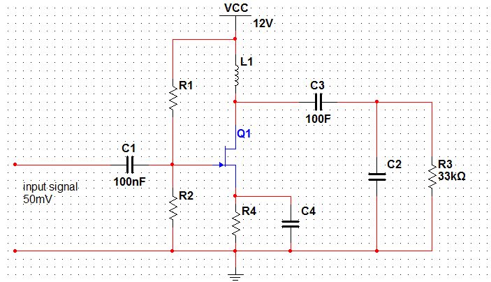
Our lecturer gaved us a semester homework. The circuit looks like below
He asked us to calculate the values. Those labeled components cannot be changed.
What really confused me is the inductor in the source channel. Both the resistor R1 & R2 looks like a voltage divider. C2 is a bypass cap. The FET looks more to me like a variable resistor. So where should i start?
The requirements are:
1. gain must be more than 20dB
2. Q factor must be above 20 and as high as possible.
3. centre frequency 680kHz from a range of 500k to 1.2M
4. input is a sine wave.
Thanks for any reply in advance! If possible please let me know the guidelines on how you calculate or is there any theory involved! Thanks!
I have a some problem encountered during my homework. I have no idea where to post it so if its not in the appropriate sub-forum please help me move it mods =)
Our lecturer gaved us a semester homework. The circuit looks like below
He asked us to calculate the values. Those labeled components cannot be changed.
What really confused me is the inductor in the source channel. Both the resistor R1 & R2 looks like a voltage divider. C2 is a bypass cap. The FET looks more to me like a variable resistor. So where should i start?
The requirements are:
1. gain must be more than 20dB
2. Q factor must be above 20 and as high as possible.
3. centre frequency 680kHz from a range of 500k to 1.2M
4. input is a sine wave.
Thanks for any reply in advance! If possible please let me know the guidelines on how you calculate or is there any theory involved! Thanks!
